ADCMP604BKSZ-REEL7

Data Sheet ADCMP604/ADCMP605
Rev. C | Page 7 of 14
PIN CONFIGURATIONS AND FUNCTION DESCRIPTIONS
ADCMP604
TOP VIEW
(Not to Scale)
Q
1
Q
6
V
EE
2
V
CCI
/V
CCO
5
V
P
3
V
N
4
05916-002
Figure 3. ADCMP604 Pin Configuration
Table 5. ADCMP604 Pin Function Descriptions (6-Lead SC70)
Pin No. Mnemonic Description
1 Q
Noninverting Output. Q is at logic high if the analog voltage at the noninverting input, V
P
, is greater than the
analog voltage at the inverting input, V
N
.
2 V
EE
Negative Supply Voltage.
3 V
P
Noninverting Analog Input.
4 V
N
Inverting Analog Input.
5 V
CCI
/V
CCO
Input Section Supply/Output Section Supply. V
CCI
and V
CCO
are shared pin.
6
Q
Inverting Output. Q is at logic low if the analog voltage at the noninverting input, V
P
, is greater than the analog
voltage at the inverting input, V
N
.
05916-003
NOTES
1. EXPOSED PAD. IF CONNECTED, THE
EPAD MUST BE CONNECTED TO V
EE
.
9
8
7
1
2
3
V
EE
LE/HYS
S
DN
V
CCO
V
CCI
V
EE
4
V
P
5
V
EE
6
V
N
12
Q
11
V
EE
10
Q
ADCMP605
TOP VIEW
(Not to Scale)
Figure 4. ADCMP605 Pin Configuration
Table 6. ADCMP605 Pin Function Descriptions (12-Lead LFCSP_WQ)
Pin No. Mnemonic Description
1 V
CCO
Output Section Supply.
2 V
CCI
Input Section Supply.
3, 5, 9, 11 V
EE
Negative Supply Voltages.
4 V
P
Noninverting Analog Input.
6 V
N
Inverting Analog Input.
7 S
DN
Shutdown. Drive this pin low to shut down the device.
8 LE/HYS Latch/Hysteresis Control. Bias with resistor or current for hysteresis; drive low to latch.
10
Q
Inverting Output. Q is at Logic low if the analog voltage at the noninverting input, V
P
, is greater than the
analog voltage at the inverting input, V
N
, if the comparator is in compare mode.
12 Q
Noninverting Output. Q is at Logic high if the analog voltage at the noninverting input, V
P
, is greater
than the analog voltage at the inverting input, V
N
, if the comparator is in compare mode.
Heat Sink Paddle V
EE
The metallic back surface of the package is electrically connected to V
EE
. It can be left floating because
Pin 3, Pin 5, Pin 9, and Pin 11 provide adequate electrical connection. It can also be soldered to the
application board if improved thermal and/or mechanical stability is desired.
EPAD Exposed Pad. If connected, the EPAD must be connected to V
EE
.
ADCMP604/ADCMP605 Data Sheet
TYPICAL PERFORMANCE CHARACTERISTICS
V
CCI
= V
CCO
= 2.5 V, T
A
= 25°C, unless otherwise noted.
CURRENT (µA)
LE/HYS PIN (V)
80
0
60
0
40
0
200
0
200
40
0
60
0
80
0
1 0
1 2
3 4
5 6
7
V
CC
= 5.5VV
CC
= 2.5V
05916-010
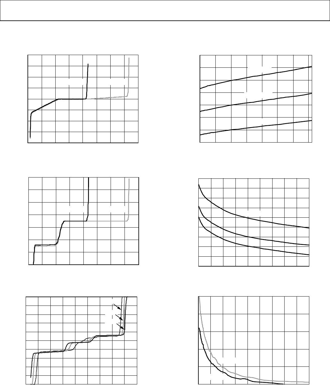
Figure 5. LE/HYS Pin Current vs. Voltage
CURRENT (µA)
S
DN
PIN (V)
150
10
0
50
0
50
100
150
200
–1 0 1
2 3 4
5 6 7
V
CC
= 5.5VV
CC
= 2.5V
05916-006
Figure 6. S
DN
Pin Current vs. Voltage
–10
–8
–6
–4
–2
0
2
4
6
8
1
0
–1.0 –0
.5 0.0 0
.5 1.0 1.
5 2.0 2.5
3.0 3.5
V
CM
AT V
CC
= 2.5V
I
B
(µA)
+125°C
–40°C
+25°C
05916-009
Figure 7. Input Bias Current vs. Input Common-Mode Voltage
0.90
1
.0
0
1.10
1.
20
1
.30
1.4
0
1.50
1
.
60
2.4 3.4 4.4 5.4
OUTPUT (V)
2.9 3.9 4.9 5.9
V
CCO
(V)
OUTPUT HI
OUTPUT LO
OUTPUT V
CM
05916-011
Figure 8. LVDS Output Level vs. V
CCO
(V)
400
450
500
550
600
650
700
750
800
850
2.40 2.80 3.20 3.60 4.00 4.40 4.80 5.20 5.60 6.00
V
CCO
(V)
RISE/FALL (ps)
+125°C
+25°C
–40°C
05916-007
Figure 9. LVDS Output Rise/Fall Time vs. V
CCO
(V)
0
50
100
150
200
250
50 100 150
200 250 300 350 400 450 500
HYSTERESIS RESISTOR (kΩ)
HYSTERESIS (mV)
V
CC
= 2.5V
V
CC
= 5.5V
05916-008
Figure 10. Hysteresis vs. Hysteresis Resistor
Rev. C | Page 8 of 14
Data Sheet ADCMP604/ADCMP605
HYS PIN CURRENTA)
HYSTERESIS (mV)
0
5
0
100
150
20
0
25
0
300
35
0
18
–1
6
14–12–10–8–6–4–20
+125°C
+25°C
–40°C
05916-012
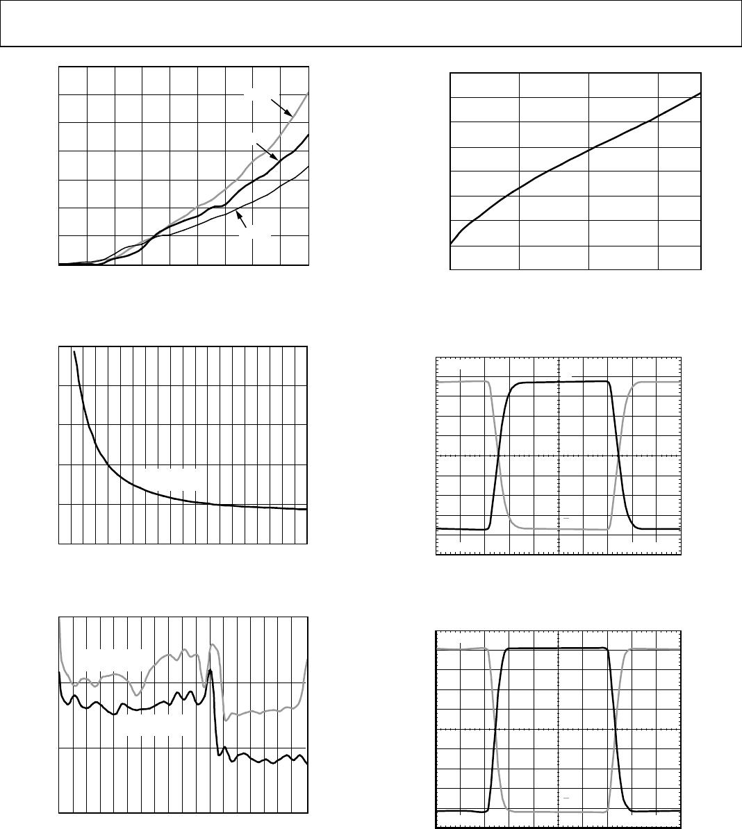
Figure 11. Hysteresis vs. HYS Pin Current
1.0
1.5
2.0
2.5
3.0
3.5
0 10 20 30 40 50 60 70 80 90 100
OVERDRIVE (mV)
PROPAGATION DELAY (ns)
PROPAGATION
DELAY
05916-004
Figure 12. Propagation Delay vs. Input Overdrive
1.3
1.4
1.5
1.6
0.6 –0.2 0.2
0.6 1.0 1
.4 1.8 2.2 2.6 3.0
V
CM
AT V
CC
(2.5V)
DELAY (ns)
PROPAGATION
DELAY RISE ns
PROPAGATION
DELAY FALL ns
05916-005
Figure 13. Propagation Delay vs. Input Common-Mode Voltage
0.36
0.37
0.38
0.39
0.40
0.41
0.42
0.43
0.44
2.4 3.4 4.4 5.4
V
CCO
(V)
OUTPUT SWING (V)
05916-013
Figure 14. LVDS Output Swing vs. V
CCO
(V)
925.0mV 2.000ns/DIV
1.425V
Q
Q
05916-014
Figure 15. 50 MHz Output Voltage Waveform at V
CCO
= 2.5 V
1.043V
2.000ns/DIV
1.543V
Q
Q
05916-015
Figure 16. 50 MHz Output Voltage Waveform at V
CCO
= 5 V
Rev. C | Page 9 of 14

ADCMP604BKSZ-REEL7

Mfr. #:
Manufacturer:
Analog Devices Inc.
Description:
Analog Comparators RR Fast 2.5-5.5V SGL-Supply LVDS
Lifecycle:
New from this manufacturer.
Delivery:
DHL FedEx Ups TNT EMS
Payment:
T/T Paypal Visa MoneyGram Western Union