REV. D–12–
AD7713
Figures 2a and 2b gives similar information to that outlined in
Table I. In this plot, the output rms noise is shown for the full
range of available cutoff frequencies rather than for some typical
cutoff frequencies as in Tables I and II. The numbers given in
these plots are typical values at 25°C.
GAIN OF 1
GAIN OF 2
GAIN OF 4
GAIN OF 8
0.1
1.0
1000.0
100.0
10.0
10000.0
10 100 1k 10
k
NOTCH FREQUENCY (Hz)
OUTPUT NOISE (V)
Figure 2a. Plot of Output Noise vs. Gain and Notch
Frequency (Gains of 1 to 8)
GAIN OF 16
GAIN OF 32
GAIN OF 64
GAIN OF 128
0.1
1.0
100.0
10.0
1000.0
10 100 1k 10
k
NOTCH FREQUENCY (Hz)
OUTPUT NOISE (V)
Figure 2b. Plot of Output Noise vs. Gain and Notch
Frequency (Gains of 16 to 128)
CIRCUIT DESCRIPTION
The AD7713 is a - ADC with on-chip digital filtering, intended
for the measurement of wide dynamic range, low frequency signals,
such as those in industrial control or process control applications. It
contains a - (or charge balancing) ADC, a calibration
microcontroller with on-chip static RAM, a clock oscillator, a
digital filter, and a bidirectional serial communications port.
The part contains three analog input channels, two program-
mable gain differential input channels, and one programmable
gain high-level single-ended input channel. The gain range on
both inputs is from 1 to 128. For the AIN1 and AIN2 inputs,
this means that the input can accept unipolar signals of between
0 mV to 20 mV and 0 V to 2.5 V or bipolar signals in the range
from ±20 mV to ±2.5 V when the reference input voltage equals
2.5 V. The input voltage range for the AIN3 input is 4 V
REF
/
GAIN and is 0 V to 10 V with the nominal reference of 2.5 V and
a ANALOG gain of 1. The input signal to the selected analog
input channel is continuously sampled at a rate determined by
the frequency of the master clock, MCLK IN, and the selected
gain (see Table III). A charge balancing ADC (- modulator)
converts the sampled signal into a digital pulse train whose duty
cycle contains the digital information. The programmable gain
function on the analog input is also incorporated in this -
modulator with the input sampling frequency being modified to
give the higher gains. A sinc
3
digital low-pass filter processes the
output of the - modulator and updates the output register at
a rate determined by the first notch frequency of this filter. The
output data can be read from the serial port randomly or peri-
odically at any rate up to the output register update rate. The
first notch of this digital filter (and therefore its –3 dB frequency)
can be programmed via an on-chip control register. The
programmable range for this first notch frequency is from
1.952 Hz to 205.59 Hz, giving a programmable range for the
–3 dB frequency of 0.52 Hz to 53.9 Hz.
The basic connection diagram for the part is shown in Figure 3.
This shows the AD7713 in the external clocking mode with
both the AV
DD
and DV
DD
pins of the AD7713 being driven
from the analog 5 V supply. Some applications will have sepa-
rate supplies for both AV
DD
and DV
DD
, and in some of these
cases, the analog supply will exceed the 5 V digital supply (see the
Power Supplies and Grounding section).
REF IN(+)
AIN1(+)
AIN1(–)
AIN3
AV
DD
DV
DD
AGND
DGND
MCLK IN
MCLK OUT
REF IN(–)
ANALOG 5V
SUPPLY
0.1F10F
AD7713
DIFFERENTIAL
ANALOG INPUT
SINGLE-ENDED
ANALOG INPUT
ANALOG
GROUND
DIGITAL
GROUND
MODE
DV
DD
STANDBY
DV
DD
AIN2(+)
AIN2(–)
2.5V
REFERENCE
DRDY
DATA
READY
TFS
TRANSMIT
(WRITE)
RFS
RECEIVE
(READ)
SDATA
SERIAL
DATA
SCLK
SERIAL
CLOCK
A0
ADDRESS
INPUT
DIFFERENTIAL
ANALOG INPUT
SYNC
Figure 3. Basic Connection Diagram
The AD7713 provides a number of calibration options that can
be programmed via the on-chip control register. A calibration
cycle can be initiated at any time by writing to this control regis-
ter. The part can perform self-calibration using the on-chip
calibration microcontroller and SRAM to store calibration
parameters. Other system components may also be included in
the calibration loop to remove offset and gain errors in the input
channel using the system calibration mode. Another option is a
background calibration mode where the part continuously
performs self-calibration and updates the calibration coeffi-
cients. Once the part is in this mode, the user does not have to
worry about issuing periodic calibration commands to the device
or asking the device to recalibrate when there is a change in the
ambient temperature or power supply voltage.
REV. D
AD7713
–13–
The AD7713 gives the user access to the on-chip calibration
registers, allowing the microprocessor to read the device’s calibra-
tion coefficients and also to write its own calibration coefficients
to the part from prestored values in E
2
PROM. This gives the
microprocessor much greater control over the AD7713’s calibra-
tion procedure. It also means that the user can verify that the
device has performed its calibration correctly by comparing the
coefficients after calibration with prestored values in E
2
PROM.
For battery-operated or low power systems, the AD7713 offers
a standby mode (controlled by the STANDBY pin) that reduces
idle power consumption to typically 150 µW.
THEORY OF OPERATION
The general block diagram of a - ADC is shown in Figure 4.
It contains the following elements:
•A sample-hold amplifier
•A differential amplifier or subtracter
•An analog low-pass filter
•A 1-bit ADC (comparator)
•A 1-bit DAC
ANALOG
LOW-PASS
FILTER
DAC
DIGITAL
FILTER
DIGITAL DATA
COMPARATOR
S/H AMP
Figure 4. General
-
ADC
In operation, the analog signal sample is fed to the subtracter,
along with the output of the 1-bit DAC. The filtered difference
signal is fed to the comparator, whose output samples the differ-
ence signal at a frequency many times that of the analog signal
sampling frequency (oversampling).
Oversampling is fundamental to the operation of - ADCs.
Using the quantization noise formula for an ADC
SNR Number of Bits dB +
()
602 176..
a 1-bit ADC or comparator yields an SNR of 7.78 dB.
The AD7713 samples the input signal at a frequency of 7.8 kHz
or greater (see Table III). As a result, the quantization noise is
spread over a much wider frequency than that of the band of
interest. The noise in the band of interest is reduced still fur-
ther by analog filtering in the modulator loop, which shapes
the quantization noise spectrum to move most of the noise
energy to frequencies outside the bandwidth of interest. The
noise performance is thus improved from this 1-bit level to the
performance outlined in Tables I and II and in Figures 2a and 2b.
The output of the comparator provides the digital input for the
1-bit DAC, so that the system functions as a negative feedback
loop that tries to minimize the difference signal. The digital data
that represents the analog input voltage is contained in the duty
cycle of the pulse train appearing at the output of the compara-
tor. It can be retrieved as a parallel binary data-word using a
digital filter.
- ADCs are generally described by the order of the analog
low-pass filter. A simple example of a first-order - ADC is
shown in Figure 5. This contains only a first-order low-pass
filter or integrator. It also illustrates the derivation of the alter-
native name for these devices: charge balancing ADCs.
COMPARATOR
DIFFERENTIAL
AMPLIFIER INTEGRATOR
+FS
–FS
DAC
V
IN
Figure 5. Basic Charge-Balancing ADC
It consists of a differential amplifier (whose output is the differ-
ence between the analog input and the output of a 1-bit DAC),
an integrator, and a comparator. The term charge balancing comes
from the fact that this system is a negative feedback loop that tries
to keep the net charge on the integrator capacitor at 0 by balanc-
ing charge injected by the input voltage with charge injected by
the 1-bit DAC. When the analog input is 0, the only contribu-
tion to the integrator output comes from the 1-bit DAC. For the
net charge on the integrator capacitor to be 0, the DAC output
must spend half its time at +FS and half its time at –FS. Assum-
ing ideal components, the duty cycle of the comparator will be 50%.
When a positive analog input is applied, the output of the 1-bit
DAC must spend a larger proportion of the time at +FS, so the
duty cycle of the comparator increases. When a negative input
voltage is applied, the duty cycle decreases.
The AD7713 uses a second-order - modulator and a digital
filter that provides a rolling average of the sampled output.
After power-up or if there is a step change in the input voltage,
there is a settling time that must elapse before valid data is
obtained.
Input Sample Rate
The modulator sample frequency for the device remains at
f
CLK IN
/512 (3.9 kHz @ f
CLK IN
= 2 MHz) regardless of the
selected gain. However, gains greater than 1 are achieved by a
combination of multiple input samples per modulator cycle and
a scaling of the ratio of the reference capacitor to input capaci-
tor. As a result of the multiple sampling, the input the sample
rate of the device varies with the selected gain (see Table III).
The effective input impedance is 1/C f
S
, where C is the input
sampling capacitance and f
S
is the input sample rate.
Table III. Input Sampling Frequency vs. Gain
Gain Input Sampling Frequency (f
S
)
1f
CLK IN
/256 (7.8 kHz @ f
CLK IN
= 2 MHz)
22 f
CLK IN
/256 (15.6 kHz @ f
CLK IN
= 2 MHz)
44 f
CLK IN
/256 (31.2 kHz @ f
CLK IN
= 2 MHz)
88 f
CLK IN
/256 (62.4 kHz @ f
CLK IN
= 2 MHz)
16 8 f
CLK IN
/256 (62.4 kHz @ f
CLK IN
= 2 MHz)
32 8 f
CLK IN
/256 (62.4 kHz @ f
CLK IN
= 2 MHz)
64 8 f
CLK IN
/256 (62.4 kHz @ f
CLK IN
= 2 MHz)
128 8 f
CLK IN
/256 (62.4 kHz @ f
CLK IN
= 2 MHz)
REV. D–14–
AD7713
DIGITAL FILTERING
The AD7713’s digital filter behaves like a similar analog filter,
with a few minor differences.
First, since digital filtering occurs after the A-to-D conversion
process, it can remove noise injected during the conversion
process. Analog filtering cannot do this.
On the other hand, analog filtering can remove noise superimposed
on the analog signal before it reaches the ADC. Digital filtering
cannot do this, and noise peaks riding on signals near full scale
have the potential to saturate the analog modulator and digital
filter, even though the average value of the signal is within limits.
To alleviate this problem, the AD7713 has overrange headroom
built into the - modulator and digital filter, which allows over-
range excursions of 5% above the analog input range. If noise
signals are larger than this, consideration should be given to analog
input filtering or to reducing the input channel voltage so that its
full scale is half that of the analog input channel full scale. This will
provide an overrange capability greater than 100% at the expense
of reducing the dynamic range by 1 bit (50%).
Filter Characteristics
The cutoff frequency of the digital filter is determined by the value
loaded to Bits FS0 to FS11 in the control register. At the maxi-
mum clock frequency of 2 MHz, the minimum cutoff frequency of
the filter is 0.52 Hz, while the maximum programmable cutoff
frequency is 53.9 Hz.
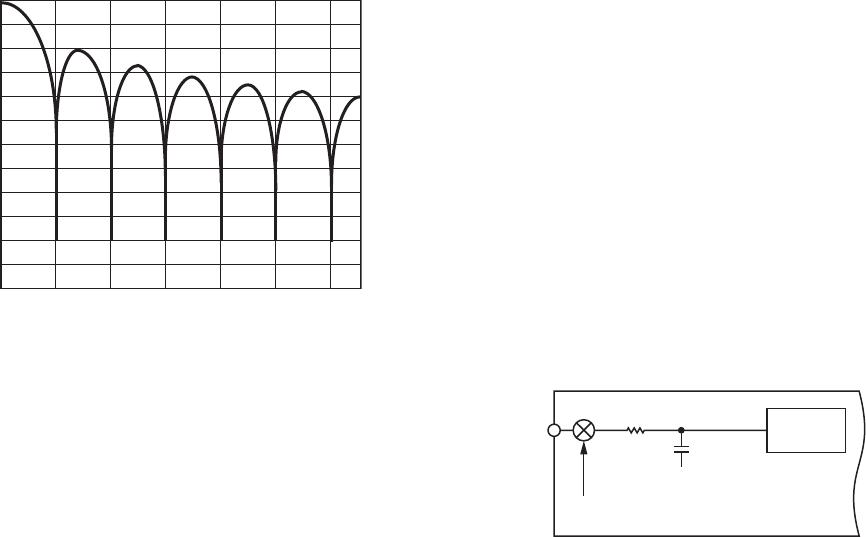
Figure 6 shows the filter frequency response for a cutoff frequency
of 0.52 Hz, which corresponds to a first filter notch frequency of
2 Hz. This is a (sinx/x)
3
response (also called sinc
3
) that provides
>100 dB of 50 Hz and 60 Hz rejection. Programming a differ-
ent cutoff frequency via FS0 to FS11 does not alter the profile
of the filter response; it changes the frequency of the notches as
outlined in the Control Register section.
–240
–180
–200
–220
–60
–80
–100
–120
–140
–160
0
–20
–40
024681012
FREQUENCY (Hz)
GAIN (dB)
Figure 6. Frequency Response of AD7713 Filter
Since the AD7713 contains this on-chip, low-pass filtering,
there is a settling time associated with step function inputs, and
data on the output will be invalid after a step change until the
settling time has elapsed. The settling time depends upon the
notch frequency chosen for the filter. The output data rate
equates to this filter notch frequency, and the settling time of
the filter to a full-scale step input is four times the output data
period. In applications using both input channels, the settling
time of the filter must be allowed to elapse before data from the
second channel is accessed.
Post Filtering
The on-chip modulator provides samples at a 3.9 kHz output
rate. The on-chip digital filter decimates these samples to
provide data at an output rate that corresponds to the pro-
grammed first notch frequency of the filter. Since the output
data rate exceeds the Nyquist criterion, the output rate for a
given bandwidth will satisfy most application requirements.
However, there may be some applications that require a higher
data rate for a given bandwidth and noise performance. Appli-
cations that need this higher data rate will require some post
filtering following the digital filter of the AD7713.
For example, if the required bandwidth is 1.57 Hz but the required
update rate is 20 Hz, the data can be taken from the AD7713 at
the 20 Hz rate giving a –3 dB bandwidth of 5.24 Hz. Post filtering
can be applied to this to reduce the bandwidth and output noise,
to the 1.57 Hz bandwidth level, while maintaining an output rate
of 20 Hz.
Post filtering can also be used to reduce the output noise from
the device for bandwidths below 0.52 Hz. At a gain of 128, the
output rms noise is 250 nV. This is essentially device noise or
white noise, and since the input is chopped, the noise has a flat
frequency response. By reducing the bandwidth below 0.52 Hz,
the noise in the resultant pass band can be reduced. A reduction
in bandwidth by a factor of 2 results in a 2 reduction in the
output rms noise. This additional filtering will result in a longer
settling time.
Antialias Considerations
The digital filter does not provide any rejection at integer
multiples of the modulator sample frequency (n 3.9 kHz,
where n = 1, 2, 3...). This means that there are frequency
bands, ±f
3
dB wide (f
3
dB is cutoff frequency selected by FS0
to FS11), where noise passes unattenuated to the output.
However, due to the AD7713’s high oversampling ratio, these
bands occupy only a small fraction of the spectrum, and most
broadband noise is filtered. In any case, because of the high
oversampling ratio, a simple, RC, single-pole filter is generally
sufficient to attenuate the signals in these bands on the analog
input and thus provide adequate antialiasing filtering.
If passive components are placed in front of the AIN1 and
AIN2 inputs of the AD7713, care must be taken to ensure that
the source impedance is low enough so as not to introduce
gain errors in the system. The dc input impedance for the
AIN1 and AIN2 inputs is over 1 G. The input appears as a
dynamic load that varies with the clock frequency and with the
selected gain (see Figure 7). The input sample rate, as shown
in Table III, determines the time allowed for the analog input
capacitor, C
IN
, to be charged. External impedances result in a
longer charge time for this capacitor, which result in gain er-
rors being introduced on the analog inputs. Both inputs of the
differential input channels look into similar input circuitry.
AIN
HIGH
IMPEDANCE
> 1G
R
INT
(7k TYP)
C
INT
(11.5pF TYP)
SWITCHING FREQUENCY DEPENDS ON
f
CLKIN
AND SELECTED GAIN
V
BIAS
Figure 7. AIN1, AIN2 Input Impedance

AD7713ARZ-REEL

Mfr. #:
Manufacturer:
Analog Devices Inc.
Description:
Analog to Digital Converters - ADC CMOS 24B w/ Matched RTD Crnt Source
Lifecycle:
New from this manufacturer.
Delivery:
DHL FedEx Ups TNT EMS
Payment:
T/T Paypal Visa MoneyGram Western Union

Products related to this Datasheet