REV. D
AD7713
–21–
DRDY line will go high, turning off the SDATA output as per
Figure 12a.
Write Operation
Data can be written to either the control register or calibration
registers. In either case, the write operation is not affected by
the DRDY line, and the write operation does not have any
effect on the status of DRDY. A write operation to the control
register or the calibration register must always write 24 bits to
the respective register.
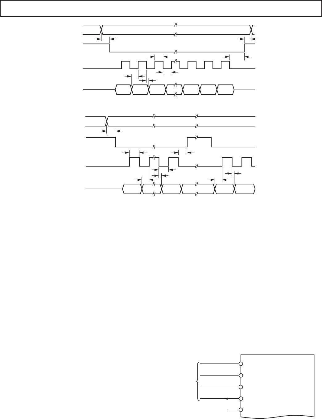
Figure 13a shows a write operation to the AD7713 with TFS
remaining low for the duration of the write operation. A0
determines whether a write operation transfers data to the con-
trol register or to the calibration registers. This A0 signal must
remain valid for the duration of the serial write operation. As
before, the serial clock line should be low between read and
write operations. The serial data to be loaded to the AD7713
must be valid on the high level of the externally applied SCLK
signal. Data is clocked into the AD7713 on the high level of this
SCLK signal with the MSB transferred first. On the last active
high time of SCLK, the LSB is loaded to the AD7713.
Figure 13b shows a timing diagram for a write operation to the
AD7713 with TFS returning high during the write operation
and returning low again to write the rest of the data-word. Tim-
ing parameters and functions are very similar to that outlined
for Figure 13a, but Figure 13b has a number of additional times
to show timing relationships when TFS returns high in the
middle of transferring a word.
Data to be loaded to the AD7713 must be valid prior to the
rising edge of the SCLK signal. TFS should return high during
the low time of SCLK. After TFS returns low again, the next bit
of the data-word to be loaded to the AD7713 is clocked in on
the next high level of the SCLK input. On the last active high
time of the SCLK input, the LSB is loaded to the AD7713.
SIMPLIFYING THE EXTERNAL CLOCKING MODE
INTERFACE
In many applications, the user may not require the facility of
writing to the on-chip calibration registers. In this case, the
serial interface to the AD7713 in external clocking mode can be
simplified by connecting the TFS line to the A0 input of the
AD7713 (see Figure 14). This means that any write to the
device will load data to the control register (since A0 is low
while TFS is low), and any read to the device will access data
from the output data register or from the calibration registers
(since A0 is high while RFS is low). It should be noted that in
this arrangement, the user does not have the capability of read-
ing from the control register. Another method of simplifying the
interface is to generate the TFS signal from an inverted RFS
signal. However, generating the signals the opposite way around
(RFS from an inverted TFS) will cause writing errors.
FOUR
INTERFACE
LINES
RFS
AD7713
SDATA
SCLK
TFS
A0
Figure 14. Simplified Interface with
TFS
Connected to A0
SCLK (I)
SDATA (I)
TFS (I)
A0 (I)
MSB
LSB
t
32
t
33
t
34
t
26
t
27
t
36
t
35
Figure 13a. External Clocking Mode, Control/Calibration Register Write Operation
SCLK (I)
SDATA (I)
TFS (I)
A0 (I)
MSB
BIT N
BIT N+1
t
32
t
26
t
30
t
27
t
36
t
35
t
35
t
36
Figure 13b. External Clocking Mode, Control/Calibration Register Write Operation
(
TFS
Returns High During Write Operation)
REV. D–22–
AD7713
MICROCOMPUTER/MICROPROCESSOR INTERFACING
The AD7713’s flexible serial interface allows easy interface to
most microcomputers and microprocessors. Figure 15 shows a
flowchart diagram for a typical programming sequence for read-
ing data from the AD7713 to a microcomputer, while Figure 16
shows a flowchart diagram for writing data to the AD7713.
Figures 17 and 18 show some typical interface circuits.
The flowchart in Figure 15 is for continuous read operations
from the AD7713 output register. In the example shown, the
DRDY line is continuously polled. Depending on the micropro-
cessor configuration, the DRDY line may come to an interrupt
input, in which case the DRDY will automatically generate an
interrupt without being polled. Reading the serial buffer could
be anything from one read operation up to three read operations
(where 24 bits of data are read into an 8-bit serial register). A
read operation to the control/calibration registers is similar, but,
in this case, the status of DRDY can be ignored. The A0 line is
brought low when the RFS line is brought low when reading
from the control register.
CONFIGURE AND
INITIALIZE C/P
SERIAL PORT
BRING RFS LOW
POLL DRDY
BRING RFS,TFS
AND HIGH
START
3
BRING RFS HIGH
READ SERIAL BUFFER
REVERSE ORDER
OF BITS
DRDY
LOW?
YES
NO
Figure 15. Flowchart for Continuous Read Operation
to the AD7713
The flowchart also shows the bits being reversed after they have
been read in from the serial port. This depends on whether the
microprocessor expects the MSB of the word first or the LSB of
the word first. The AD7713 outputs the MSB first.
The flowchart in Figure 16 is for a single 24-bit write operation
to the AD7713 control or calibration registers. This shows data
being transferred from data memory to the accumulator before
being written to the serial buffer. Some microprocessor systems
will allow data to be written directly to the serial buffer from data
memory. Writing data to the serial buffer from the accumulator
will generally consist of either two or three write operations,
depending on the size of the serial buffer.
The flowchart also shows the option of the bits being reversed
before being written to the serial buffer. This depends on whether
the first bit transmitted by the microprocessor is the MSB or the
LSB. The AD7713 expects the MSB as the first bit in the data
stream. In cases where the data is being read or being written in
bytes and the data has to be reversed, the bits will have to be
reversed for every byte.
CONFIGURE AND
INITIALIZE C/P
SERIAL PORT
BRING RFS AND A0 LOW
BRING RFS,TFS
AND A0 HIGH
START
END
3
LOAD DATA FROM
ADDRESS TO
ACCUMULATOR
WRITE DATA FROM
ACCUMULATOR TO
SERIAL BUFFER
BRING TFS AND A0 HIGH
REVERSE ORDER
OF BITS
Figure 16. Flowchart for Single Write Operation to
the AD7713
AD7713 to 8XC51 Interface
Figure 17 shows an interface between the AD7713 and the 8XC51
microcontroller. The AD7713 is configured for its external clock-
ing mode, while the 8XC51 is configured in its Mode 0 serial
interface mode. The DRDY line from the AD7713 is connected to
the Port P1.2 input of the 8XC51, so the DRDY line is polled by
the 8XC51. The DRDY line can be connected to the INT1 input
of the 8XC51 if an interrupt driven system is preferred.
RFS
AD7713
SDATA
SCLK
TFS
A0
P1.0
P3.0
P3.1
P1.1
P1.2
MODE
DRDY
P1.3
SYNC
DV
DD
8XC51
Figure 17. AD7713 to 8XC51 Interface
REV. D
AD7713
–23–
Table V shows some typical 8XC51 code used for a single 24-bit
read from the output register of the AD7713. Table V shows
some typical code for a single write operation to the control
register of the AD7713. The 8XC51 outputs the LSB first in a
write operation while the AD7713 expects the MSB first, so the
data to be transmitted has to be rearranged before being written
to the output serial register. Similarly, the AD7713 outputs the
MSB first during a read operation while the 8XC51 expects the
LSB first. Therefore, the data which is read into the serial buffer
needs to be rearranged before the correct data-word from the
AD7713 is available in the accumulator.
Table V. 8XC51 Code for Reading from the AD7713
MOV SCON,#00010001B; Configure 8051 for MODE 0
MOV IE,#00010000B; Disable All Interrupts
SETB 90H; Set P1.0, Used as RFS
SETB 91H; Set P1.1, Used as TFS
SETB 93H; Set P1.3, Used as A0
MOV R1,#003H; Sets Number of Bytes to Be Read
in A Read Operation
MOV R0,#030H; Start Address for Where Bytes
Will Be Loaded
MOV R6,#004H; Use P1.2 as DRDY
WAIT:
NOP;
MOV A,P1; Read Port 1
ANL A,R6; Mask Out All Bits Except DRDY
JZ READ; If Zero Read
SJMP WAIT; Otherwise Keep Polling
READ:
CLR 90H; Bring RFS Low
CLR 98H; Clear Receive Flag
POLL:
JB 98H, READ1 Tests Receive Interrupt Flag
SJMP POLL
READ 1:
MOV A,SBUF; Read Buffer
RLC A; Rearrange Data
MOV B.0,C; Reverse Order of Bits
RLC A; MOV B.1,C; RLC A; MOV B.2,C;
RLC A; MOV B.3,C; RLC A; MOV B.4,C;
RLC A; MOV B.5,C; RLC A; MOV B.6,C;
RLC A; MOV B.7,C;
MOV A,B;
MOV @R0,A; Write Data to Memory
INC R0; Increment Memory Location
DEC R1 Decrement Byte Counter
MOV A,R1
JZ END Jump if Zero
JMP WAIT Fetch Next Byte
END:
SETB 90H Bring RFS High
FIN:
SJMP FIN
Table VI. 8XC51 Code for Writing to the AD7713
MOV SCON,#00000000B; Configure 8051 for MODE 0
Operation and Enable Serial
Reception
MOV IE,#10010000B; Enable Transmit Interrupt
MOV IP,#00010000B; Prioritize the Transmit Interrupt
SETB 91H; Bring TFS High
SETB 90H; Bring RFS High
MOV R1,#003H; Sets Number of Bytes to Be
Written in a Write Operation
MOV R0,#030H; Start Address in RAM for Bytes
MOV A,#00H; Clear Accumulator
MOV SBUF,A; Initialize the Serial Port
WAIT:
JMP WAIT; Wait for Interrupt
INT ROUTINE:
NOP; Interrupt Subroutine
MOV A,R1; Load R1 to Accumulator
JZ FIN; If Zero Jump to FIN
DEC R1; Decrement R1 Byte Counter
MOV A,@R; Move Byte into the Accumulator
INC R0; Increment Address
RLC A; Rearrange Data—From LSB
First to MSB First
MOV B.0,C; RLC A; MOV B.1,C; RLC A;
MOV B.2,C; RLC A; MOV B.3,C; RLC A;
MOV B.4,C; RLC A; MOV B.5,C; RLC A;
MOV B.6,C; RLC A: MOV B.7,C; MOV A,B;
CLR 93H; Bring A0 Low
CLR 91H; Bring TFS Low
MOV SBUF,A; Write to Serial Port
RETI; Return from Subroutine
FIN:
SETB 91H; Set TFS High
SETB 93H; Set A0 High
RETI; Return from Interrupt Subroutine
AD7713 to 68HC11 Interface
Figure 18 shows an interface between the AD7713 and the
68HC11 microcontroller. The AD7713 is configured for its exter-
nal clocking mode, while the SPI port is used on the 68HC11,
which is in its single chip mode. The DRDY line from the AD7713
is connected to the Port PC2 input of the 68HC11, so the DRDY
line is polled by the 68HC11. The DRDY line can be connected to
the IRQ input of the 68HC11 if an interrupt driven system is
preferred. The 68HC11 MOSI and MISO lines should be config-
ured for wired-OR operation. Depending on the interface
configuration, it may be necessary to provide bidirectional buffers
between the 68HC11 MOSI and MISO lines.
The 68HC11 is configured in the master mode with its CPOL
bit set to a Logic 0 and its CPHA bit set to a Logic 1.
AD7713ARZ-REEL

Mfr. #:
Manufacturer:
Analog Devices Inc.
Description:
Analog to Digital Converters - ADC CMOS 24B w/ Matched RTD Crnt Source
Lifecycle:
New from this manufacturer.
Delivery:
DHL FedEx Ups TNT EMS
Payment:
T/T Paypal Visa MoneyGram Western Union

Products related to this Datasheet