REV. D–24–
AD7713
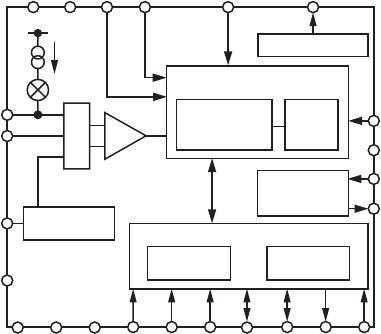
SYNC
RFS
TFS
A0
SDATA
SCLK
MODE
PC0
PC1
PC2
PC3
MISO
MOSI
68HC11 AD7713
DRDY
SS
SCK
DV
DD
DV
DD
Figure 18. AD7713 to 68HC11 Interface
APPLICATIONS
4-Wire RTD Configurations
Figure 19 shows a 4-wire RTD application where the RTD
transducer is interfaced directly to the AD7713. In the 4-wire
configuration, there are no errors associated with lead resis-
tances as no current flows in the measurement leads connected
to AIN1(+) and AIN1(–). One of the RTD current sources is
used to provide the excitation current for the RTD. A common
nominal resistance value for the RTD is 100 Ω and, therefore, the
RTD will generate a 20 mV signal, which can be handled directly
by the analog input of the AD7713. In the circuit shown, the
second RTD excitation current is used to generate the reference
voltage for the AD7713. This reference voltage is developed
across R
REF
and applied to the differential reference inputs. For
the nominal reference voltage of 2.5 V, R
REF
is 12.5 kΩ. This
scheme ensures that the analog input voltage span remains
ratiometric to the reference voltage. Any errors in the analog
input voltage due to the temperature drift of the RTD current
source is compensated for by the variation in the reference volt-
age. The typical matching between the two RTD current sources
is less than 3 ppm/°C.
AIN1(+)
AIN1(–)
AV
DD
AGND
DGND
A = 1 – 128
AD7713
RTD1
REF IN(+)
REF IN(–)
RTD2
200A
5V
R
REF
INTERNAL
CIRCUITRY
DV
DD
PGA
200A
RTD
Figure 19. 4-Wire RTD Application with the AD7713
3-Wire RTD Configurations
Figure 20 shows a 3-wire RTD configuration using the AD7713.
In the 3-wire configuration, the lead resistances will result in
errors if only one current source is used as the 200 µA will flow
through RL1 developing a voltage error between AIN1(+) and
AIN1(–). In the scheme outlined below, the second RTD cur-
rent source is used to compensate for the error introduced by
the 200 µA flowing through RL1. The second RTD current
flows through RL2. Assuming RL1 and RL2 are equal (the leads
would normally be of the same material and of equal length) and
RTD1 and RTD2 match, then the error voltage across RL2 equals
the error voltage across RL1, and no error voltage is developed
between AIN1(+) and AIN1(–). Twice the voltage is developed
across RL3 but since this is a common-mode voltage, it will not
introduce any errors. The reference voltage is derived from one
of the current sources. This gives all the benefits of eliminating
RTD temperature coefficient errors as outlined in Figure 19.
The voltage on either RTD input can go to within 2 V of the
AV
DD
supply. The circuit is shown for a 2.5 V reference.
AIN(+)
AIN(–)
AV
DD
DV
DD
AGND
DGND
A = 1 – 128
AD7713
RTD1
RTD2
12.5k⍀
INTERNAL
CIRCUITRY
REF IN(+)
REF IN(–)
R
L1
R
L2
R
L3
PGA
RTD
200A
200A
Figure 20. 3-Wire RTD Application with the AD7713
4–20 mA Loop
The AD7713’s high level input can be used to measure the
current in 4–20 mA loop applications as shown in Figure 21. In
this case, the system calibration capabilities of the AD7713 can
be used to remove the offset caused by the 4 mA flowing through
the 500 Ω resistor. The AD7713 can handle an input span as
low as 3.2 ⫻ V
REF
(= 8 V with a V
REF
of 2.5 V) even though the
nominal input voltage range for the input is 10 V. Therefore,
the full span of the ADC can be used for measuring the current
between 4 and 20 mA.
REF IN(+)
AIN1(+)
AIN1(–)
AIN3
AGND DGND
A = 1 – 128
REF IN(–)
AD7713
4–20mA
LOOP
ANALOG 5V SUPPLY
500⍀
VOLTAGE
ATTENUATION
AV
DD
AV
DD
DV
DD
INTERNAL
CIRCUITRY
MUX
PGA
1A
Figure 21. 4-20 mA Measurement Using the AD7713