1
Microsemi Corporation
Copyright 2012, Microsemi Corporation. All Rights Reserved.
Features
Inputs/Outputs
Accepts two differential or single-ended inputs
LVPECL, LVDS, CML, HCSL, LVCMOS
Glitch-free switching of references
On-chip input termination and biasing for AC
coupled inputs
Six precision LVDS outputs
Operating frequency up to 750 MHz
Power
Option for 2.5 V or 3.3 V power supply
Current consumption of 97 mA
On-chip Low Drop Out (LDO) Regulator for superior
power supply rejection
Performance
Ultra low additive jitter of 165 fs RMS
Applications
General purpose clock distribution
Low jitter clock trees
Logic translation
Clock and data signal restoration
Redundant clock distribution
Wired communications: OTN, SONET/SDH, GE,
10
GE, FC and 10G FC
Wireless communications
High performance micro-processor clock
distribution
November 2012
Figure 1 - Functional Block Diagram
clk0_p
clk0_n
ctrl0
vt0
sel
Termination
and Bias
clk1_p
clk1_n
ctrl1
vt1
Termination
and Bias
Control
out5_p
out5_n
out4_p
out4_n
out3_p
out3_n
out2_p
out2_n
out1_p
out1_n
out0_p
out0_n
Buffer
ZL40221
Precision 2:6 LVDS Fanout Buffer with Glitch-
free Input Reference Switching
and On-Chip Input Termination
Data Sheet
Ordering Information
ZL40221LDG1 32 Pin QFN Trays
ZL40221LDF1 32 Pin QFN Tape and Reel
Matte Tin
Package size: 5 x 5 mm
-40
o
C to +85
o
C
ZL40221 Data Sheet
Table of Contents
2
Microsemi Corporation
Features . . . . . . . . . . . . . . . . . . . . . . . . . . . . . . . . . . . . . . . . . . . . . . . . . . . . . . . . . . . . . . . . . . . . . . . . . . . . . . . . . 1
Applications . . . . . . . . . . . . . . . . . . . . . . . . . . . . . . . . . . . . . . . . . . . . . . . . . . . . . . . . . . . . . . . . . . . . . . . . . . . . . 1
1.0 Package Description . . . . . . . . . . . . . . . . . . . . . . . . . . . . . . . . . . . . . . . . . . . . . . . . . . . . . . . . . . . . . . . . . . . . 4
2.0 Pin Description. . . . . . . . . . . . . . . . . . . . . . . . . . . . . . . . . . . . . . . . . . . . . . . . . . . . . . . . . . . . . . . . . . . . . . . . . 5
3.0 Functional Description . . . . . . . . . . . . . . . . . . . . . . . . . . . . . . . . . . . . . . . . . . . . . . . . . . . . . . . . . . . . . . . . . . 6
3.1 Clock Inputs. . . . . . . . . . . . . . . . . . . . . . . . . . . . . . . . . . . . . . . . . . . . . . . . . . . . . . . . . . . . . . . . . . . . . . . . . 6
3.1.1 Clock Input Selection . . . . . . . . . . . . . . . . . . . . . . . . . . . . . . . . . . . . . . . . . . . . . . . . . . . . . . . . . . . . . 6
3.1.2 Clock Input Terminations . . . . . . . . . . . . . . . . . . . . . . . . . . . . . . . . . . . . . . . . . . . . . . . . . . . . . . . . . . 7
3.2 Clock Outputs . . . . . . . . . . . . . . . . . . . . . . . . . . . . . . . . . . . . . . . . . . . . . . . . . . . . . . . . . . . . . . . . . . . . . . 12
3.3 Device Additive Jitter . . . . . . . . . . . . . . . . . . . . . . . . . . . . . . . . . . . . . . . . . . . . . . . . . . . . . . . . . . . . . . . . . 15
3.4 Power Supply . . . . . . . . . . . . . . . . . . . . . . . . . . . . . . . . . . . . . . . . . . . . . . . . . . . . . . . . . . . . . . . . . . . . . . 16
3.4.1 Sensitivity to power supply noise . . . . . . . . . . . . . . . . . . . . . . . . . . . . . . . . . . . . . . . . . . . . . . . . . . . 16
3.4.2 Power supply filtering . . . . . . . . . . . . . . . . . . . . . . . . . . . . . . . . . . . . . . . . . . . . . . . . . . . . . . . . . . . . 16
3.4.3 PCB layout considerations . . . . . . . . . . . . . . . . . . . . . . . . . . . . . . . . . . . . . . . . . . . . . . . . . . . . . . . . 16
4.0 AC and DC Electrical Characteristics . . . . . . . . . . . . . . . . . . . . . . . . . . . . . . . . . . . . . . . . . . . . . . . . . . . . . 17
5.0 Performance Characterization . . . . . . . . . . . . . . . . . . . . . . . . . . . . . . . . . . . . . . . . . . . . . . . . . . . . . . . . . . . 19
6.0 Typical Behavior . . . . . . . . . . . . . . . . . . . . . . . . . . . . . . . . . . . . . . . . . . . . . . . . . . . . . . . . . . . . . . . . . . . . . . 20
7.0 Package Characteristics . . . . . . . . . . . . . . . . . . . . . . . . . . . . . . . . . . . . . . . . . . . . . . . . . . . . . . . . . . . . . . . 21
8.0 Mechanical Drawing . . . . . . . . . . . . . . . . . . . . . . . . . . . . . . . . . . . . . . . . . . . . . . . . . . . . . . . . . . . . . . . . . . . 22
ZL40221 Data Sheet
List of Figures
3
Microsemi Corporation
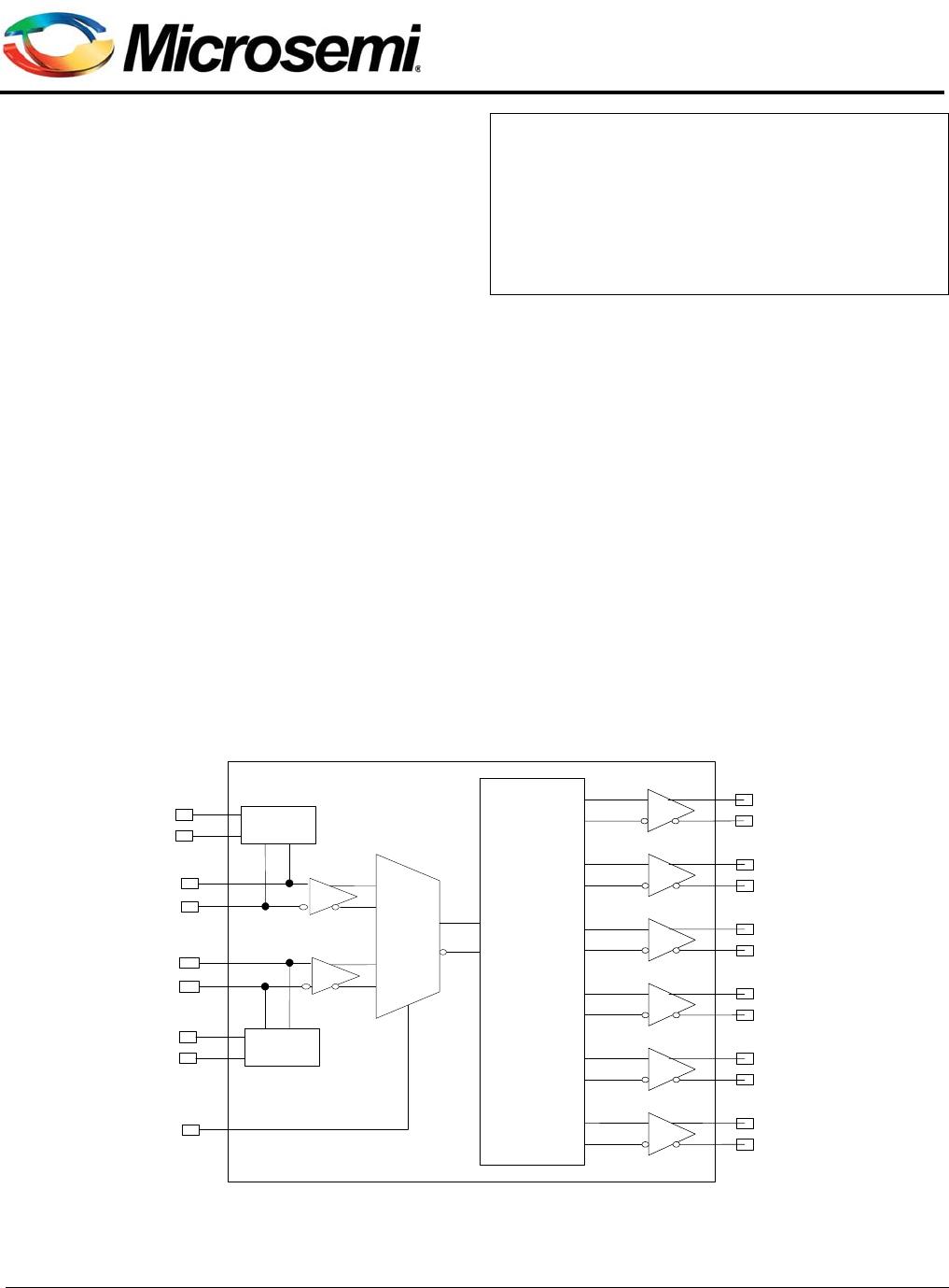
Figure 1 - Functional Block Diagram . . . . . . . . . . . . . . . . . . . . . . . . . . . . . . . . . . . . . . . . . . . . . . . . . . . . . . . . . . . . 1
Figure 2 - Pin Connections . . . . . . . . . . . . . . . . . . . . . . . . . . . . . . . . . . . . . . . . . . . . . . . . . . . . . . . . . . . . . . . . . . . 4
Figure 3 - Simplified Diagram of input stage . . . . . . . . . . . . . . . . . . . . . . . . . . . . . . . . . . . . . . . . . . . . . . . . . . . . . . 6
Figure 4 - Output During Clock Switch - Both Clocks Running . . . . . . . . . . . . . . . . . . . . . . . . . . . . . . . . . . . . . . . . 7
Figure 5 - Clock Input - LVPECL - DC Coupled . . . . . . . . . . . . . . . . . . . . . . . . . . . . . . . . . . . . . . . . . . . . . . . . . . . . 7
Figure 6 - Clock Input - LVPECL - AC Coupled . . . . . . . . . . . . . . . . . . . . . . . . . . . . . . . . . . . . . . . . . . . . . . . . . . . . 8
Figure 7 - Clock Input - LVDS - DC Coupled . . . . . . . . . . . . . . . . . . . . . . . . . . . . . . . . . . . . . . . . . . . . . . . . . . . . . . 8
Figure 8 - Clock Input - LVDS - AC Coupled . . . . . . . . . . . . . . . . . . . . . . . . . . . . . . . . . . . . . . . . . . . . . . . . . . . . . . 9
Figure 9 - Clock Input - CML- AC Coupled . . . . . . . . . . . . . . . . . . . . . . . . . . . . . . . . . . . . . . . . . . . . . . . . . . . . . . . 9
Figure 10 - Clock Input - HCSL- AC Coupled . . . . . . . . . . . . . . . . . . . . . . . . . . . . . . . . . . . . . . . . . . . . . . . . . . . . 10
Figure 11 - Clock Input - AC-coupled Single-Ended . . . . . . . . . . . . . . . . . . . . . . . . . . . . . . . . . . . . . . . . . . . . . . . 10
Figure 12 - Clock Input - DC-coupled 3.3V CMOS . . . . . . . . . . . . . . . . . . . . . . . . . . . . . . . . . . . . . . . . . . . . . . . . 11
Figure 13 - Simplified LVDS Output Driver. . . . . . . . . . . . . . . . . . . . . . . . . . . . . . . . . . . . . . . . . . . . . . . . . . . . . . . 12
Figure 14 - LVDS DC Coupled Termination (Internal Receiver Termination) . . . . . . . . . . . . . . . . . . . . . . . . . . . . . 12
Figure 15 - LVDS DC Coupled Termination (External Receiver Termination) . . . . . . . . . . . . . . . . . . . . . . . . . . . . 13
Figure 16 - LVDS AC Coupled Termination . . . . . . . . . . . . . . . . . . . . . . . . . . . . . . . . . . . . . . . . . . . . . . . . . . . . . . 13
Figure 17 - LVDS AC Output Termination for CML Inputs . . . . . . . . . . . . . . . . . . . . . . . . . . . . . . . . . . . . . . . . . . . 14
Figure 18 - Additive Jitter . . . . . . . . . . . . . . . . . . . . . . . . . . . . . . . . . . . . . . . . . . . . . . . . . . . . . . . . . . . . . . . . . . . . 15
Figure 19 - Decoupling Connections for Power Pins . . . . . . . . . . . . . . . . . . . . . . . . . . . . . . . . . . . . . . . . . . . . . . . 16
Figure 20 - Differential Voltage Parameter. . . . . . . . . . . . . . . . . . . . . . . . . . . . . . . . . . . . . . . . . . . . . . . . . . . . . . . 18
Figure 21 - Input To Output Timing . . . . . . . . . . . . . . . . . . . . . . . . . . . . . . . . . . . . . . . . . . . . . . . . . . . . . . . . . . . . 18

ZL40221LDF1

Mfr. #:
Manufacturer:
Microchip / Microsemi
Description:
Clock Buffer 2:6 LVDS Fanout Buffer w/Int. Term.
Lifecycle:
New from this manufacturer.
Delivery:
DHL FedEx Ups TNT EMS
Payment:
T/T Paypal Visa MoneyGram Western Union

Products related to this Datasheet