ZL40221 Data Sheet
6
Microsemi Corporation
3.0 Functional Description
he ZL40221 is an LVDS clock fanout buffer with six output clock drivers capable of operating at frequencies up to
750MHz.
The ZL40221 provides an internal input termination netwo
rk for DC and AC coupled inputs; optional input biasing
for AC coupled inputs is also provided. The ZL40221 can accept DC or AC coupled LVPECL and LVDS input
signals, AC coupled CML or HCSL input signals, and single ended signals. A pin compatible device with external
termination is also available.
The ZL40221 is designed to fan out
low-jitter reference clocks for wired or optical communications applications
while adding minimal jitter to the clock signal. An internal linear power supply regulator and bulk capacitors
minimize additive jitter due to power supply noise. The device operates from 2.5V+/-5% or 3.3V+/-5% supply. Its
operation is guaranteed over the industrial temperature range -40°C to +85°C.
The device block diagram is shown in Figure 1; its operation is described in the following sections.
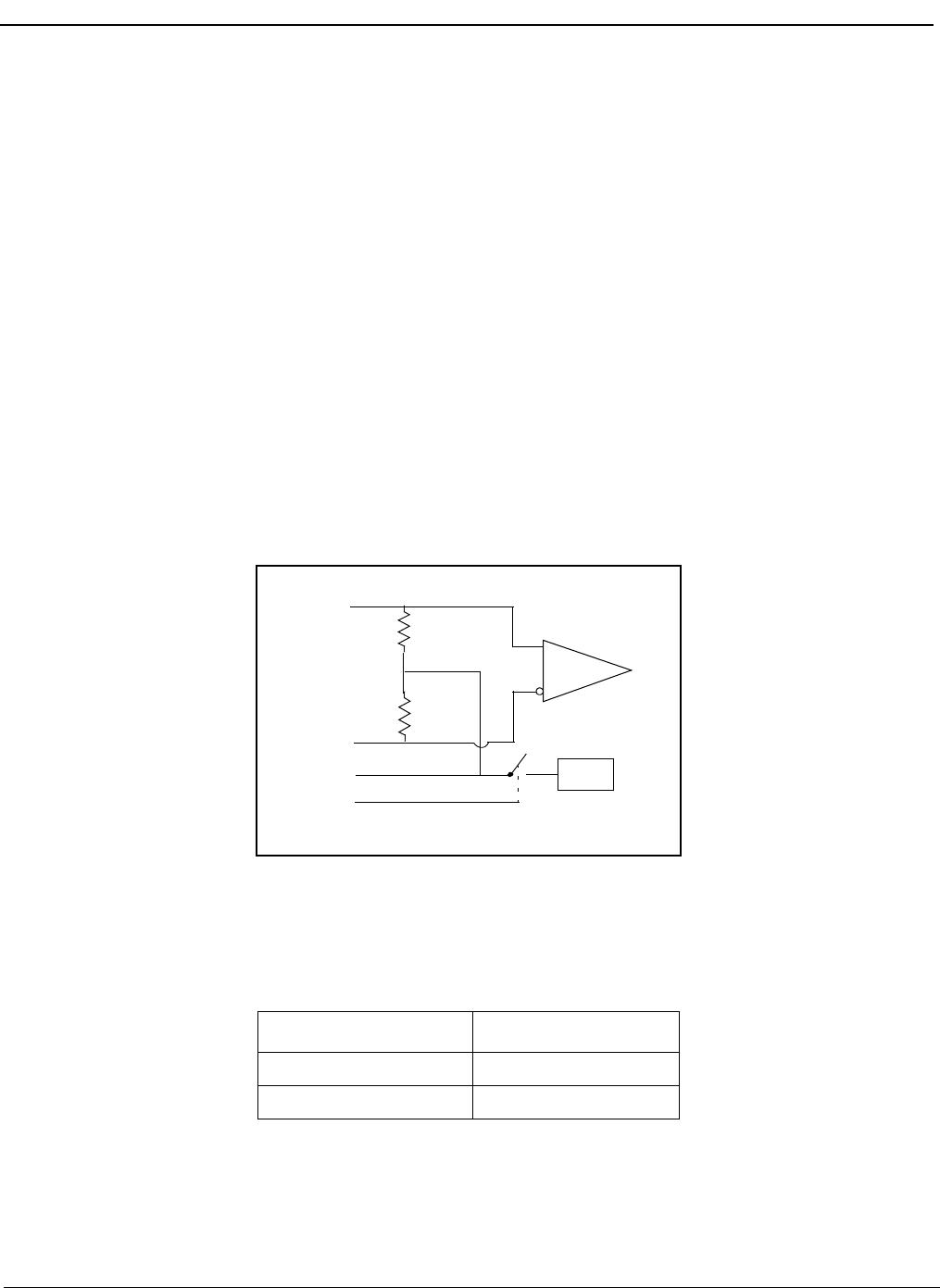
3.1 Clock Inputs
The device has a differential input equipped with two on-chip 50 Ohm termination resistors arranged in series with a
center tap. The input can accept many differential and single-ended signals with AC or DC coupling as appropriate.
A control pin is available to enable internal biasing for AC coupled inputs. A block diagram of the input stage is in
Figure 3.
Receiver
clk_n
50
clk_p
Vt
50
Bias
ctrl
Figure 3 - Simplified Diagram of input stage
3.1.1 Clock Input Selection
The select line chooses which input clock is routed to the outputs.
Table 1 - Input Selection
Sel Active Input
0 clk0
1 clk1
The following figure shows the expected clock
switching performance. The output stops at the first falling edge of
the initial clock after the select pin changes state. During switching there will be a short time when the output clock
is not toggling. After this delay, the output will start toggling again with a rising edge of the newly selected clock.
This behavior is independent of the frequencies of the input clocks. For instance, the two clocks could be at
different frequencies and the behavior would still be consistent with this figure.