ZL40221 Data Sheet
15
Microsemi Corporation
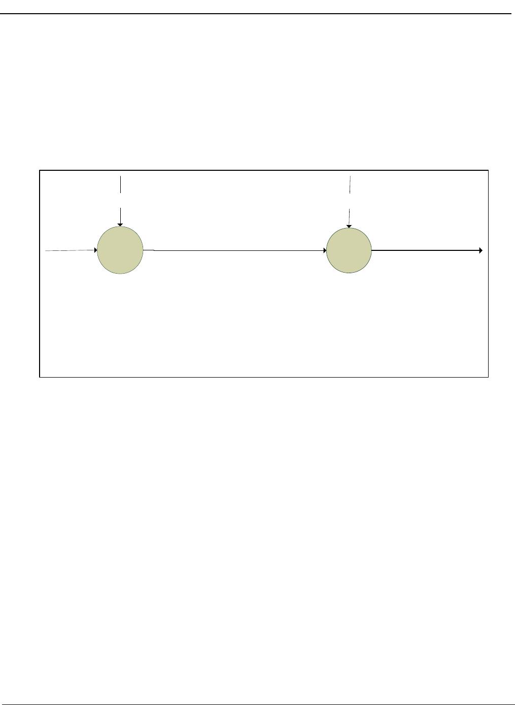
3.3 Device Additive Jitter
The ZL40221 clock fanout buffer is not intended to filter clock jitter. The jitter performance of this type of device is
characterized by its additive jitter. Additive jitter is the jitter the device would add to a hypothetical jitter-free clock as
it passes through the device. The additive jitter of the ZL40221 is random and as such it is not correlated to the jitter
of the input clock signal.
The square of the resultant random RMS jitter at the output
of the ZL40221 is equal to the sum of the squares of the
various random RMS jitter sources including: input clock jitter; additive jitter of the buffer; and additive jitter due to
power supply noise. There may be additional deterministic jitter sources, but they are not shown in Figure 18.
+
J
in
2
J
add
2
J
ps
2
J
in
= Random input clock jitter (RMS)
J
add
= Additive jitter due to the device (RMS)
J
ps
= Additive jitter due to power supply noise (RMS)
J
out
= Resultant random output clock jitter (RMS)
+
J
out
2
= J
in
2
+J
add
2
+J
ps
2
Figure 18 - Additive Jitter