2 µs
clk0
clk1
sel
outn
1
0
ZL40221 Data Sheet
7
Microsemi Corporation
Figure 4 - Output During Clock Switch - Both Clocks Running
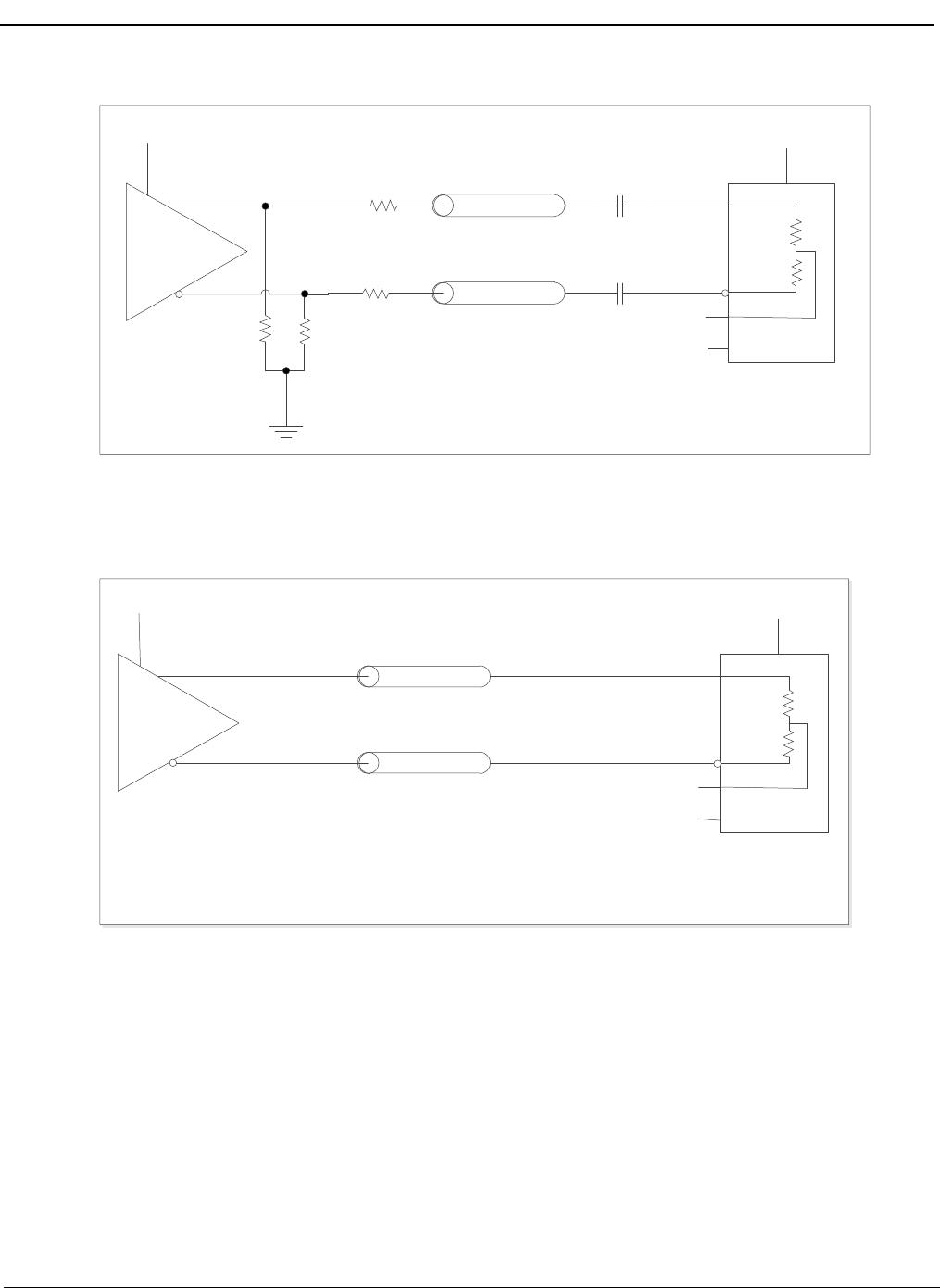
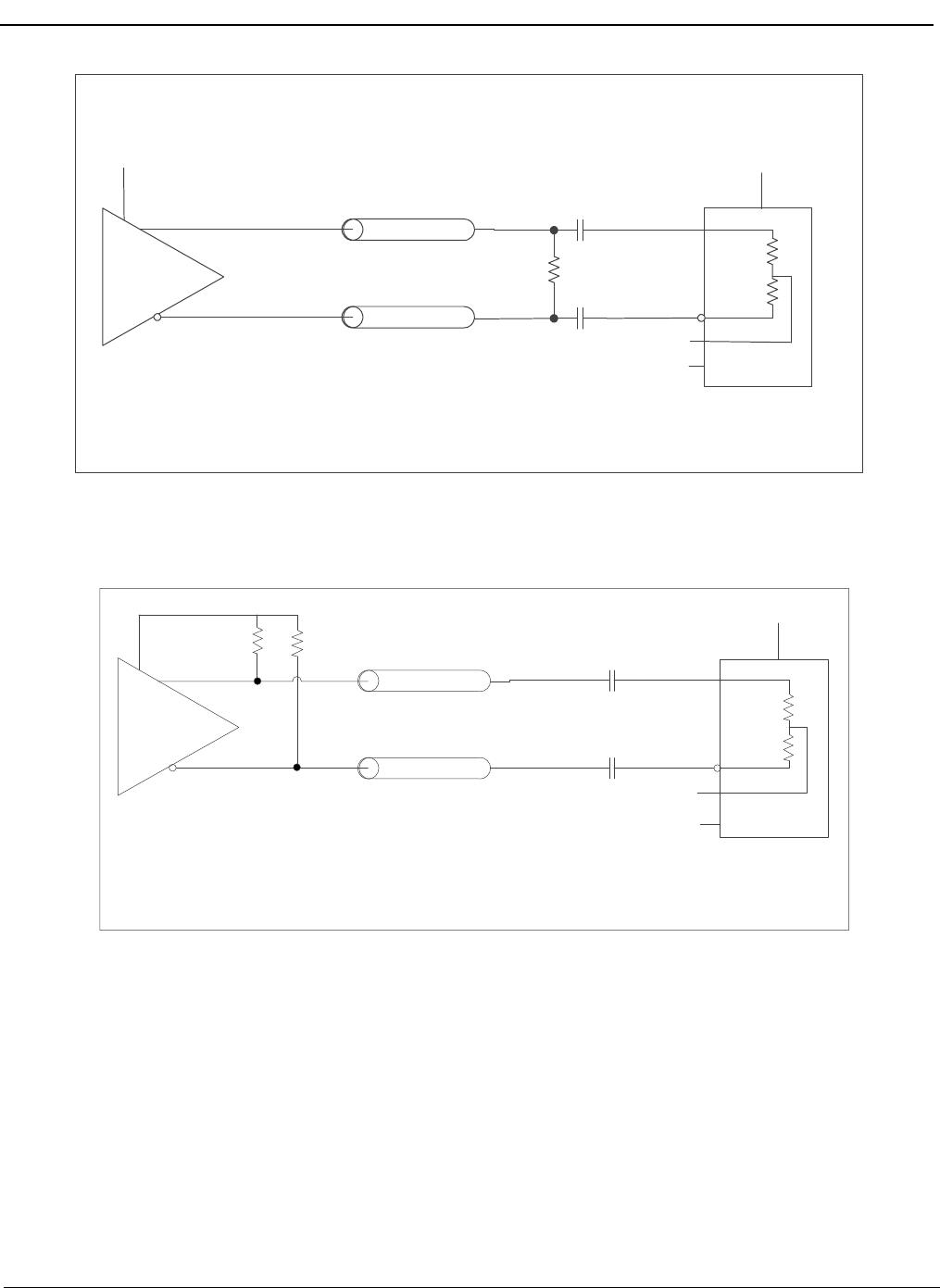
3.1.2 Clock Input Terminations
This following figures give the components values and configuration for the various circuits compatible with the
input stage and the use of the Vt and ctrl pins in each case.
In the following diagrams were the ct
rl pin is ’1’ and the Vt pin is not connected, the Vt pin can be instead connected
to V
DD
with a capacitor. A capacitor can also help in Figure 5 between Vt and V
DD
. This capacitor will minimize the
noise at the point between the two internal termination resistor
s and improve the overall performance of the device.
LVPECL
Driver
R
VDD_driver
VDD
Z
o
= 50 Ohms
Z
o
= 50 Ohms
l
k
_
p
l
k
_
n
V
t
C
t
r
l
clk_p
clk_n
Vt
Ctrl
“0”
For 3.3 V: R= 50 Ohms
For 2.5 V: R= 22 Ohms
22 Ohms
22 Ohms
Figure 5 - Clock Input - LVPECL - DC Coupled
LVPECL
Driver
VDD_driver
VDD
Z
o
= 50 Ohms
Z
o
= 50 Ohms
clk_p
clk_n
Vt
Ctrl
“1”
For 3.3 V: R= 150 Ohms
For 2.5 V: R= 85 Ohms
NC
RR
22 Ohms
22 Ohms
LVDS
Driver
VDD_driver
VDD
Z
o
= 50 Ohms
Z
o
= 50 Ohms
clk_p
clk_n
Vt
Ctrl
“0”
NC
ZL40221 Data Sheet
8
Microsemi Corporation
Figure 6 - Clock Input - LVPECL - AC Coupled
Figure 7 -
Clock Input - LVDS - DC Coupled
LVDS
Driver
VDD_driver
VDD
Z
o
= 50 Ohms
Z
o
= 50 Ohms
clk_p
clk_n
Vt
Ctrl
“1”
NC
R
For VDD_driver = 3.3 V: R= 900 Ohms
For VDD_driver = 2.5 V: R = 680 Ohms
Note: This R is only needed to provide a DC
path for the LVDS driver. See driver data
sheet for more information.
CML
Driver
VDD_driver
VDD
Z
o
= 50 Ohms
Z
o
= 50 Ohms
clk_p
clk_n
Vt
Ctrl
“1”
R= 50 Ohms
NC
RR
ZL40221 Data Sheet
9
Microsemi Corporation
Figure 8 - Clock Input - LVDS - AC Coupled
Figure 9 -
Clock Input - CML- AC Coupled

ZL40221LDF1

Mfr. #:
Manufacturer:
Microchip / Microsemi
Description:
Clock Buffer 2:6 LVDS Fanout Buffer w/Int. Term.
Lifecycle:
New from this manufacturer.
Delivery:
DHL FedEx Ups TNT EMS
Payment:
T/T Paypal Visa MoneyGram Western Union

Products related to this Datasheet