11©2017 Integrated Device Technology, Inc. December 1, 2017
9ZML1233E / 9ZML1253E Datasheet
Notes for PCIe Filtered Phase Jitter tables:
1
Applies to all differential outputs when driven by 9SQL495x or equivalent, guaranteed by design and characterization.
2
Calculated from Intel-supplied clock jitter tool, when driven by 9SQL495x or equivalent with spread on and off.
3
Sample size of at least 100K cycles. This figure extrapolates to 108ps pk-pk at 1M cycles for a BER of 1
–12
.
4
For RMS values, additive jitter is calculated by solving the following equation for b [b = sqrt(c
2
- a
2
)] where “a” is rms input jitter and
“c” is rms total jitter.
5
IR is the new name for Separate Reference Independent Spread (SRIS) and Separate Reference no Spread (SRNS) PCIe clock
architectures. According to the PCIe Base Specification Rev4.0 version 0.7 draft, the jitter transfer functions and corresponding jitter
limits are not defined for the IR clock architecture. Widely accepted industry limits using widely accepted industry filters are used to
populate this table. There are no accepted filters or limits for IR clock architectures at PCIe Gen1 or Gen4 data rates.
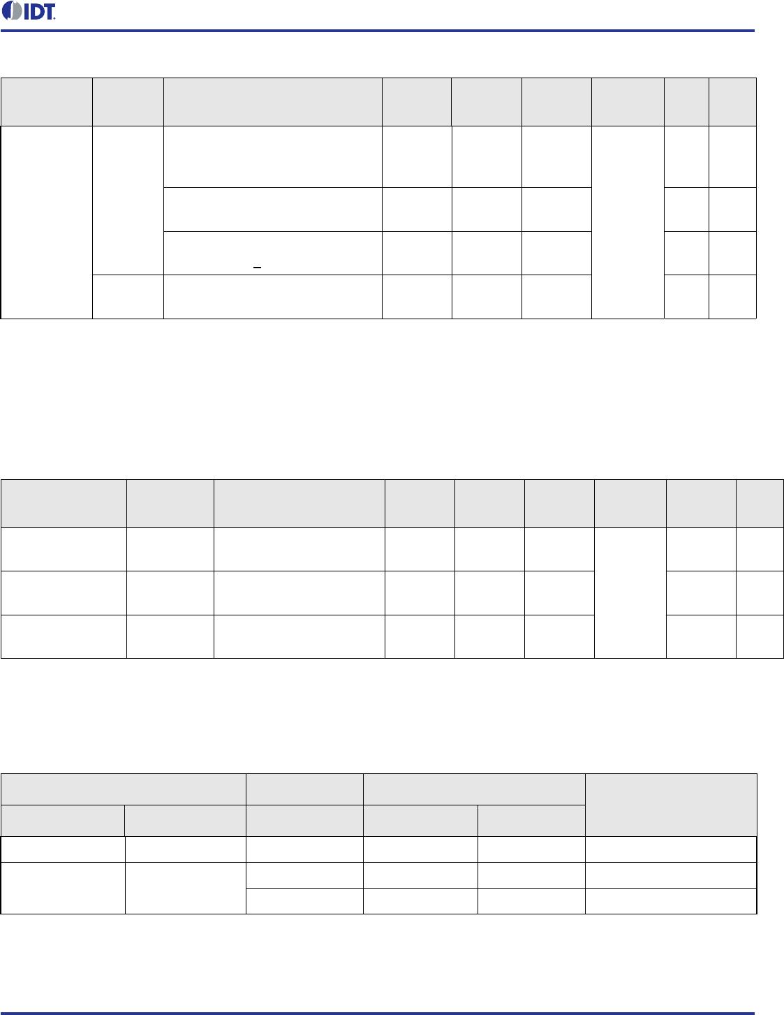
Table 10. Filtered Phase Jitter Parameters - PCIe Independent Reference (IR) Architectures
Parameter Symbol Conditions Minimum Typical Maximum
Industry
Limits
Units Notes
Phase Jitter,
PLL Mode
t
jphPCIeG2-SRIS
PCIe Gen 2
(PLL BW of 16MHz, CDR = 5MHz).
0.8 1.2 2
ps
(rms)
1, 2, 5
t
jphPCIeG3-SRIS
PCIe Gen 3
(PLL BW of 2–4MHz, CDR =
10MHz).
0.64 0.68 0.7
ps
(rms)
1, 2, 5
Additive
Phase Jitter,
Bypass Mode
t
jphPCIeG2-SRIS
PCIe Gen 2
(PLL BW of 16MHz, CDR = 5MHz).
0.00 0.02
Not
Applicable
ps
(rms)
2, 4, 5
t
jphPCIeG3-SRIS
PCIe Gen 3
(PLL BW of 2–4MHz, CDR =
10MHz).
0.00 0.02
ps
(rms)
2, 4, 5
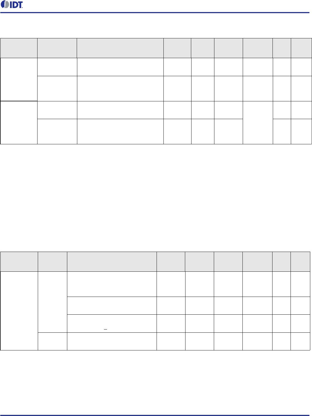
Table 11. Filtered Phase Jitter Parameters – QPI/UPI
Parameter Symbol Conditions Minimum Typical Maximum
Industry
Limits
Units Notes
Phase Jitter,
PLL Mode
t
jphQPI_UPI
QPI & UPI
(100MHz or 133MHz, 4.8Gb/s,
6.4Gb/s 12UI).
0.15 0.3 0.5
ps
(rms)
1, 2
QPI & UPI
(100MHz, 8.0Gb/s, 12UI).
0.08 0.1 0.3
ps
(rms)
1, 2
QPI & UPI
(100MHz, >
9.6Gb/s, 12UI).
0.07 0.1 0.2
ps
(rms)
1, 2
t
jphIF-UPI
IF-UPI.
0.1
0.17
0.15
0.2
1
ps
(rms)
1, 4,
5