13©2017 Integrated Device Technology, Inc. December 1, 2017
9ZML1233E / 9ZML1253E Datasheet
Power Connections (9ZML12xxE)
Power Connections (for pin-compatibility with 9ZML12xxB)
PLL Operating Mode
Note: PLL is off in Bypass Mode.
Skew Programming
Pin Number
Description
V
DD
V
DDIO
GND
1 2 Analog PLL
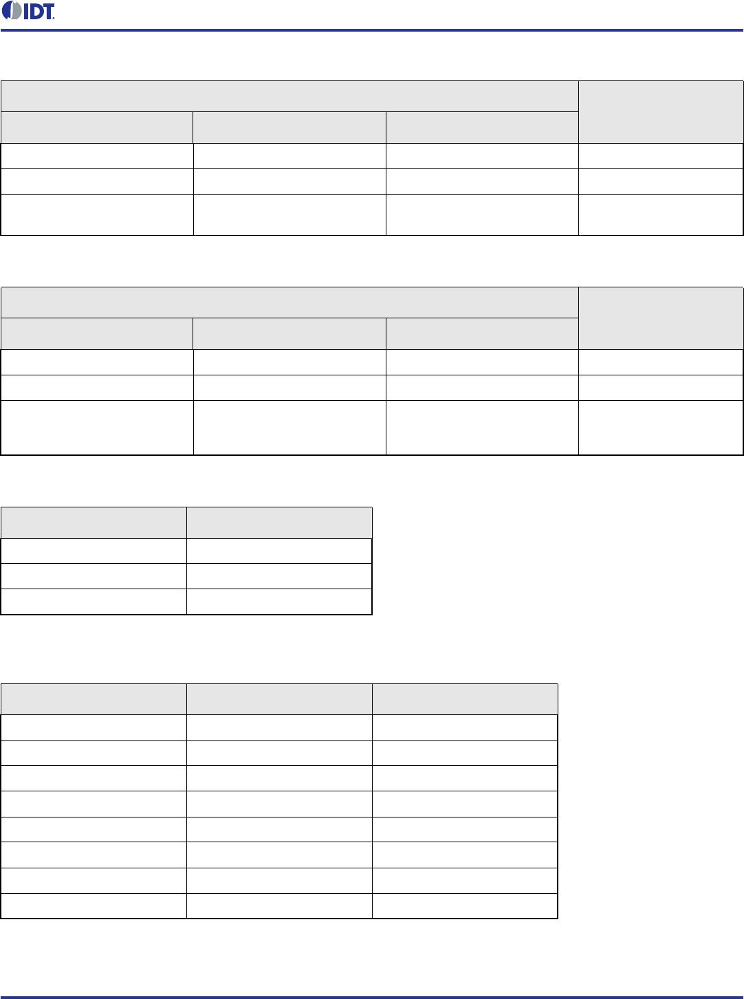
9 8 Analog input
28, 45, 64 40, 52 22, 27, 34, 39, 46, 51, 58, 63, 70 DIF clocks
Pin Number
Description
V
DD
V
DDIO
GND
1 2 Analog PLL
9 8 Analog input
28, 45, 64 21, 33, 40, 52, 57, 69
16, 22, 27, 34, 39, 46, 51, 58,
63, 70
DIF clocks
HIBW_BYPM_LOBW# Byte0[7:6]
Low (PLL Low BW) 00
Mid (Bypass) 01
High (PLL High BW) 11
Skew[2:0] Skew Steps Skew (ps)
000 0 0
001 1 -416.67
010 2 -833.33
011 3 -1250.00
100 4 -1666.67
101 5 -2083.33
110 6 -2500.00
111 7 -2916.67