24AA65/24LC65/24C65
DS21073K-page 10 © 2008 Microchip Technology Inc.
5.7 Security Options
The 24XX65 has a sophisticated mechanism for write
protecting portions of the array. This write-protect
function is programmable and allows the user to protect
0-15 contiguous 4K blocks. The user sets the security
option by sending to the device the starting block
number for the protected region and the number of
blocks to be protected. All parts will come from the
factory in the default configuration with the starting
block number set to 15 and the number of protected
blocks set to zero. THE SECURITY OPTION CAN BE
SET ONLY ONCE WITH A LENGTH GREATER THAN
ZERO.
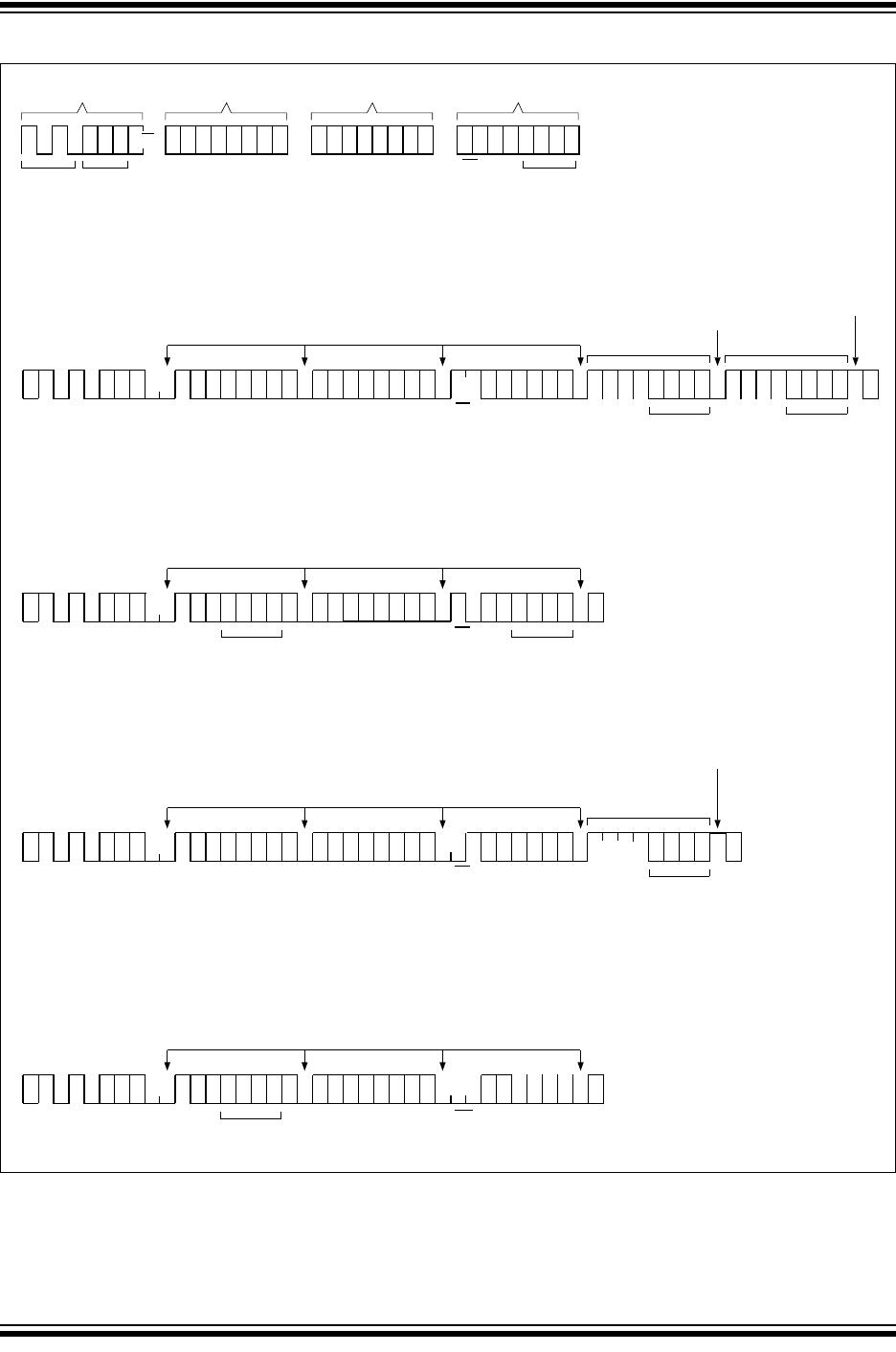
To invoke the security option, a Write command is sent
to the device with the leading bit (bit 7) of the first
address byte set to a ‘1’ (Figure 8-1). Bits 1-4 of the first
address byte define the starting block number for the
protected region.
For example, if the starting block number is to be set to
5, the first address byte would be 1XX0101X. Bits 0, 5
and 6 of the first address byte are disregarded by the
device and can be either high or low. The device will
acknowledge after the first address byte. A byte of
“don’t care” bits is then sent by the master, with the
device acknowledging afterwards. The third byte sent
to the device has bit 7 (S/HE) set high and bit 6 (R) set
low. Bits 4 and 5 are “don’t cares” and bits 0-3 define
the number of blocks to be write-protected. For exam-
ple, if three blocks are to be protected, the third byte
would be 10XX0011. After the third byte is sent to the
device, it will acknowledge and a Stop bit is then sent
by the master to complete the command.
If one of the security blocks coincides with the high
endurance block, the high endurance setting will take
precedence. Also, if the range of the security blocks
encompass the high endurance block when the secu-
rity option is set, the security block range will be set
accordingly, but the high endurance block will continue
to retain the high endurance setting. As a result, the
memory blocks preceding the high endurance block will
be set as secure sections.
During a normal write sequence, if an attempt is made
to write to a protected address, no data will be written
and the device will not report an error or abort the
command. If a Write command is attempted across a
secure boundary, unprotected addresses will be written
and protected addresses will not.
5.8 Security Configuration Read
The status of the secure portion of memory can be read
by using the same technique as programming this
option except the read bit (bit 6) of the configuration
byte is set to a one. After the configuration byte is sent,
the device will acknowledge and then send two bytes of
data to the master just as in a normal read sequence.
The master must acknowledge the first byte and not
acknowledge the second, and then send a Stop bit to
end the sequence. The upper four bits of both of these
bytes will always be read as ‘1’s. The lower four bits of
the first byte contains the starting secure block. The
lower four bits of the second byte contains the number
of secure blocks. The default starting secure block is
fifteen and the default number of secure blocks is zero
(Figure 8-1).
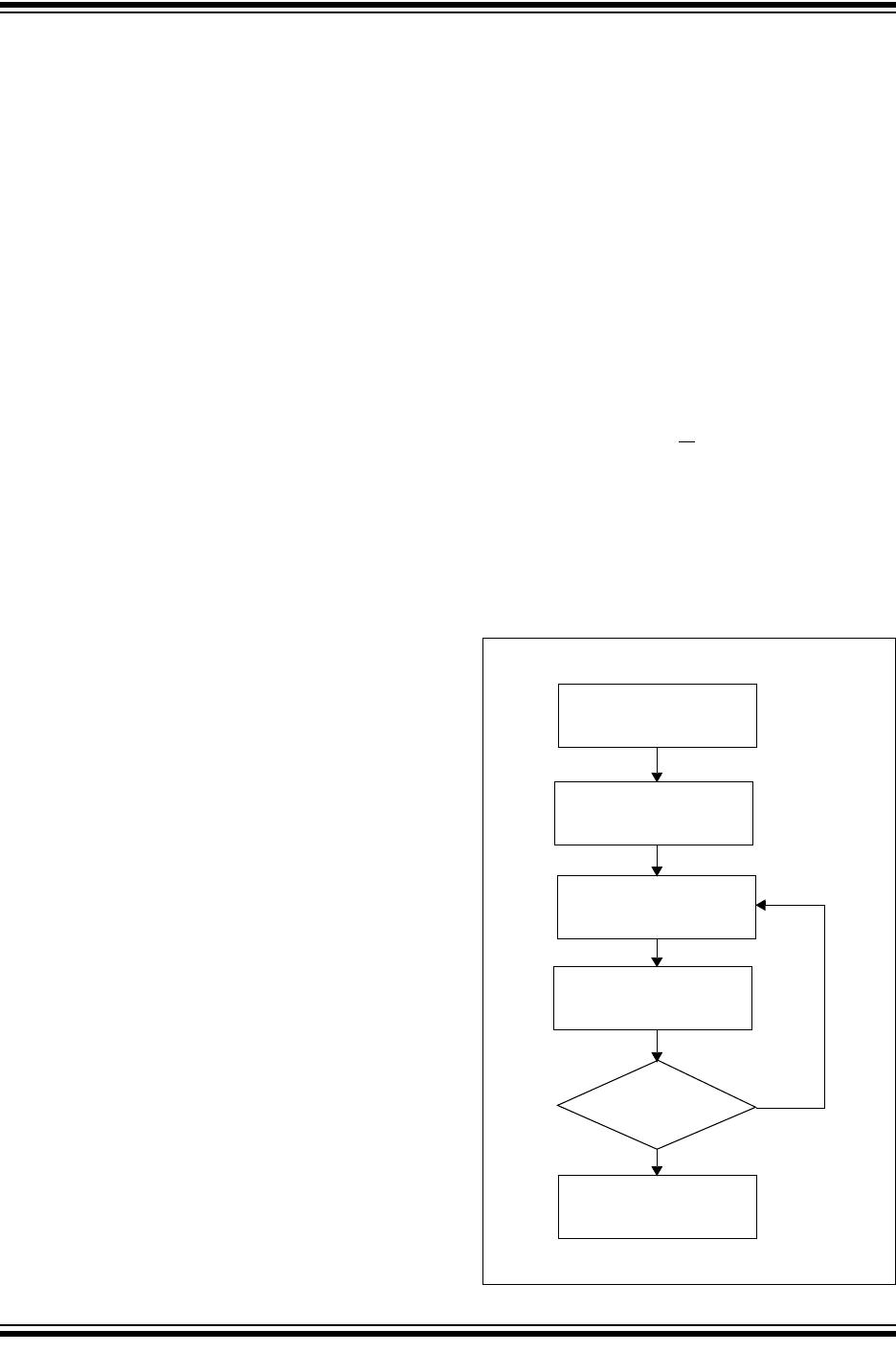
6.0 ACKNOWLEDGE POLLING
Since the device will not acknowledge during a write
cycle, this can be used to determine when the cycle is
complete (this feature can be used to maximize bus
throughput). Once the Stop condition for a Write
command has been issued from the master, the device
initiates the internally timed write cycle. ACK polling
can be initiated immediately. This involves the master
sending a Start condition followed by the control byte
for a Write command (R/W
= 0). If the device is still
busy with the write cycle, then no ACK will be returned.
If the cycle is complete, then the device will return the
ACK and the master can then proceed with the next
Read or Write command. See Figure 6-1 for flow
diagram.
FIGURE 6-1: ACKNOWLEDGE
POLLING FLOW
© 2008 Microchip Technology Inc. DS21073K-page 11
24AA65/24LC65/24C65
7.0 PAGE CACHE AND ARRAY
MAPPING
The cache is a 64-byte (8 pages x 8 bytes) FIFO buffer.
The cache allows the loading of up to 64 bytes of data
before the write cycle is actually begun, effectively
providing a 64-byte burst write at the maximum bus
rate. Whenever a Write command is initiated, the cache
starts loading and will continue to load until a Stop bit is
received to start the internal write cycle. The total
length of the write cycle will depend on how many
pages are loaded into the cache before the Stop bit is
given. Maximum cycle time for each page is 5 ms. Even
if a page is only partially loaded, it will still require the
same cycle time as a full page. If more than 64 bytes of
data are loaded before the Stop bit is given, the
Address Pointer will ‘wrap around’ to the beginning of
cache page 0 and existing bytes in the cache will be
overwritten. The device will not respond to any
commands while the write cycle is in progress.
7.1 Cache Write Starting at a Page
Boundary
If a Write command begins at a page boundary
(address bits A2, A1 and A0 are zero), then all data
loaded into the cache will be written to the array in
sequential addresses. This includes writing across a
4K block boundary. In the example shown below,
(Figure 8-2) a Write command is initiated starting at
byte 0 of page 3 with a fully loaded cache (64 bytes).
The first byte in the cache is written to byte 0 of page 3
(of the array), with the remaining pages in the cache
written to sequential pages in the array. A write cycle is
executed after each page is written. Since the write
begins at page 3 and 8 pages are loaded into the
cache, the last 3 pages of the cache are written to the
next row in the array.
7.2 Cache Write Starting at a
Non-Page Boundary
When a Write command is initiated that does not begin
at a page boundary (i.e., address bits A2, A1 and A0
are not all zero), it is important to note how the data is
loaded into the cache, and how the data in the cache is
written to the array. When a Write command begins, the
first byte loaded into the cache is always loaded into
page 0. The byte within page 0 of the cache where the
load begins is determined by the three Least Significant
Address bits (A2, A1, A0) that were sent as part of the
Write command. If the Write command does not start at
byte 0 of a page and the cache is fully loaded, then the
last byte(s) loaded into the cache will roll around to
page 0 of the cache and fill the remaining empty bytes.
If more than 64 bytes of data are loaded into the cache,
data already loaded will be overwritten. In the example
shown in Figure 8-3, a Write command has been
initiated starting at byte 2 of page 3 in the array with a
fully loaded cache of 64 bytes. Since the cache started
loading at byte 2, the last two bytes loaded into the
cache will ‘roll over' and be loaded into the first two
bytes of page 0 (of the cache). When the Stop bit is
sent, page 0 of the cache is written to page 3 of the
array. The remaining pages in the cache are then
loaded sequentially to the array. A write cycle is
executed after each page is written. If a partially loaded
page in the cache remains when the Stop bit is sent,
only the bytes that have been loaded will be written to
the array.
7.3 Power Management
The design incorporates a power Standby mode when
not in use and automatically powers off after the normal
termination of any operation when a Stop bit is received
and all internal functions are complete. This includes
any error conditions (i.e., not receiving an Acknowl-
edge or Stop condition per the two-wire bus specifica-
tion). The device also incorporates V
DD monitor
circuitry to prevent inadvertent writes (data corruption)
during low voltage conditions. The VDD monitor circuitry
is powered off when the device is in Standby mode in
order to further reduce power consumption.
8.0 PIN DESCRIPTIONS
8.1 A0, A1, A2 Chip Address Inputs
The A0..A2 inputs are used by the 24XX65 for multiple
device operation and conform to the two-wire bus
standard. The levels applied to these pins define the
address block occupied by the device in the address
map. A particular device is selected by transmitting the
corresponding bits (A2, A1, A0) in the control byte
(Figure 3-2 and Figure 8-1).
8.2 SDA Serial Address/Data Input/
Output
This is a bidirectional pin used to transfer addresses
and data into and data out of the device. It is an open
drain terminal, therefore the SDA bus requires a pull-up
resistor to V
CC (typical 10 KΩ for 100 kHz, 2 KΩ for 400
kHz).
For normal data transfer SDA is allowed to change only
during SCL low. Changes during SCL high are
reserved for indicating the Start and Stop conditions.
8.3 SCL Serial Clock
This input is used to synchronize the data transfer from
and to the device.
24AA65/24LC65/24C65
DS21073K-page 12 © 2008 Microchip Technology Inc.
FIGURE 8-1: CONTROL SEQUENCE BIT ASSIGNMENTS
A
1
Control Byte
A
2
A
0
R/W
0101
A
10
Address Byte 1
A
11
A
9
A
8
00S
A
7
A
0
Address Byte 0
Slave
Address
Device
Select
Bits
A
12
B
2
Configuration Byte
B
3
B
1
B
0
XR
X
Block
Count
S/HE
A
1
A
2
A
0
0101
X
XXX
XX1
X
Starting Block
Number
S
t
a
r
t
0
X
XXX
XX
X
X
A
C
K
X
XXX
X11
X
A
C
K
B
2
B
3
B
1
B
0
111
1
N
2
N
3
N
1
N
0
111
1
Number of
Blocks to
Protect
S
t
o
p
A
C
K
No
ACK
Data from Device
Acknowledge
from
Master
Data from Device
Acknowledges from Device
A
1
A
2
A
0
0101
B
1
B
2
B
0
X
XX1
B
3
S
t
a
r
t
0
X
XXX
XX
X
X
N
2
N
3
N
1
N
0
X01
X
A
C
K
S
t
o
p
Acknowledges from Device
A
1
A
2
A
0
A
C
K
0101
X
XXX
XX1
X
High Endurance
Block Number
S
t
a
r
t
0
X
XXX
XX
X
X
A
C
K
X
XXX
X10
X
A
C
K
B
2
B
3
B
1
B
0
111
1
S
t
o
p
A
C
K
No
ACK
Data from Device
Acknowledges from Device
A
1
A
2
A
0
A
C
K
0101
B
1
B
2
B
0
X
XX1
B
3
S
t
a
r
t
0
X
XXX
XX
X
X
A
C
K
0
000
X00
X
A
C
K
S
t
o
p
A
C
K
Acknowledges from Device
Starting Block
Number
Number of
Blocks to
Protect
R
S/HE
R
S/HE
R
S/HE
R
S/HE
Security Read
Security Write
High Endurance Block Read
High Endurance Block Write
A
C
K
A
C
K
A
C
K
A
C
K
A
C
K
High Endurance
Block Number

24LC65/SM

Mfr. #:
Manufacturer:
Microchip Technology
Description:
EEPROM 8kx8 2.5V Smart
Lifecycle:
New from this manufacturer.
Delivery:
DHL FedEx Ups TNT EMS
Payment:
T/T Paypal Visa MoneyGram Western Union