24AA65/24LC65/24C65
DS21073K-page 6 © 2008 Microchip Technology Inc.
3.6 Device Addressing
A control byte is the first byte received following the
Start condition from the master device. The control byte
consists of a four-bit control code, for the 24XX65 this
is set as ‘1010’ binary for read and write operations.
The next three bits of the control byte are the device
select bits (A2, A1, A0). They are used by the master
device to select which of the eight devices are to be
accessed. These bits are in effect the three Most
Significant bits of the word address. The last bit of the
control byte defines the operation to be performed.
When set to a one a read operation is selected, when
set to a zero a write operation is selected. The next two
bytes received define the address of the first data byte
(Figure 4-1). Because only A12..A0 are used, the
upper three address bits must be zeros. The Most
Significant bit of the Most Significant Byte is transferred
first. Following the Start condition, the 24XX65
monitors the SDA bus checking the device type
identifier being transmitted. Upon receiving a ‘1010’
code and appropriate device select bits, the slave
device (24XX65) outputs an Acknowledge signal on the
SDA line. Depending upon the state of the R/W
bit, the
24XX65 will select a read or write operation.
FIGURE 3-2: CONTROL BYTE
ALLOCATION
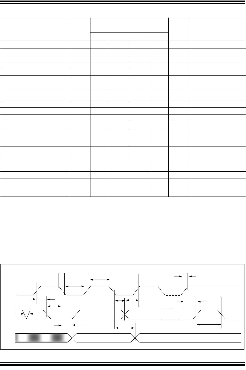
4.0 WRITE OPERATION
4.1 Byte Write
Following the Start condition from the master, the con-
trol code (four bits), the device select (three bits), and
the R/W bit which is a logic low, is placed onto the bus
by the master transmitter. This indicates to the
addressed slave receiver (24XX65) that a byte with a
word address will follow after it has generated an
Acknowledge bit during the ninth clock cycle. There-
fore, the next byte transmitted by the master is the
high-order byte of the word address and will be written
into the Address Pointer of the 24XX65. The next byte
is the Least Significant Address Byte. After receiving
another Acknowledge signal from the 24XX65, the
master device will transmit the data word to be written
into the addressed memory location. The 24XX65
acknowledges again and the master generates a Stop
condition. This initiates the internal write cycle, and
during this time the 24XX65 will not generate
Acknowledge signals (Figure 4-1).
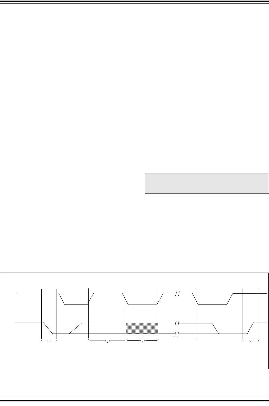
4.2 Page Write
The write control byte, word address and the first data
byte are transmitted to the 24XX65 in the same way as
in a byte write. But instead of generating a Stop
condition, the master transmits up to eight pages of
eight data bytes each (64 bytes total), which are
temporarily stored in the on-chip page cache of the
24XX65. They will be written from the cache into the
EEPROM array after the master has transmitted a Stop
condition. After the receipt of each word, the six lower
order Address Pointer bits are internally incremented by
one. The higher order seven bits of the word address
remain constant. If the master should transmit more
than eight bytes prior to generating the Stop condition
(writing across a page boundary), the address counter
(lower three bits) will roll over and the pointer will be
incremented to point to the next line in the cache. This
can continue to occur up to eight times or until the cache
is full, at which time a Stop condition should be
generated by the master. If a Stop condition is not
received, the cache pointer will roll over to the first line
(byte 0) of the cache, and any further data received will
overwrite previously captured data. The Stop condition
can be sent at any time during the transfer. As with the
byte write operation, once the Stop condition is received
an internal write cycle will begin. The 64-byte cache will
continue to capture data until a Stop condition occurs or
the operation is aborted (Figure 4-2).
Operation Control Code Device Select R/W
Read 1010 Device Address 1
Write 1010 Device Address 0
SLAVE ADDRESS
1010A2 A1 A0
R/W A
START READ/WRITE