DS564F2 13
CS5341
Confidential Draft
3/11/08
2. PIN DESCRIPTION
Pin Name # Pin Description
M0
M1
1
16
Mode Selection (Input) - Determines the operational mode of the device.
MCLK 2 Master Clock (Input) - Clock source for the delta-sigma modulator and digital filters.
VL 3 Logic Power (Input) - Positive power for the digital input/output.
SDOUT 4 Serial Audio Data Output (Output) - Output for two’s complement serial audio data.
GND 5,14 Ground (Input) - Ground reference. Must be connected to analog ground.
VD 6 Digital Power (Input) - Positive power supply for the digital section.
SCLK 7 Serial Clock (Input/Output) - Serial clock for the serial audio interface.
LRCK 8
Left Right Clock (Input/Output) - Determines which channel, Left or Right, is currently
active on the serial audio data line.
RST
9 Reset (Input) - The device enters a low power mode when low.
AINL
AINR
10
12
Analog Input (Input) - The full-scale analog input level is specified in the Analog Charac-
teristics specification table.
VQ 11
Quiescent Voltage (Output) - Filter connection for the internal quiescent
reference voltage.
VA 13 Analog Power (Input) - Positive power supply for the analog section.
FILT+ 15
Positive Voltage Reference (Output) - Positive reference voltage for the internal
sampling circuits.
M0 M1
MCLK FILT+
VL REF_GND
SDOUT VA
GND AINR
VD VQ
SCLK AINL
LRCK RST
1
2
3
4
5
6
7
8
5
1
2
6
16
15
14
13
12
11
10
9
1
2
3
4
5
6
7
8
5
1
2
6
16
15
14
13
12
11
10
9
14 DS564F2
CS5341
Confidential Draft
3/11/08
3. TYPICAL CONNECTION DIAGRAM
FILT+
V
0.1
µ
F
A/D CONVERTER
SCLK
CS5341
MCLK
VQ
1
µ
F
+
RST
VA
L
1
µ
F
1.8 V to 5V
1
µ
F
+
+
SDOUT
GND
LRCK
Power Down
and Mode
Settings
Audio Data
Processor
Timing Logic
and Clock
0.1
µ
F
0.1
µ
F
0.1
µ
F
REFGND
F
+
AINL
AINR
3.3V to 5V
1
µ
F
+
0.1
µ
F
3.3V to 5V
5.1
V
D
0.1
µ
F
10k
VL or GND
* Pull-up to VL for I
2
S
Pull-down to GND for LJ
*
M0
M1
Analog Input Buffer
Figure 21
**
** Resistor may only be
used if VD is derived from
VA. If used, do not drive
any other logic from VD
***
*** Capacitor value affects
low frequency distortion
performance as described
in Section 4.8
DS564F2 15
CS5341
Confidential Draft
3/11/08
4. APPLICATIONS
4.1 Single-, Double-, and Quad-Speed Modes
The CS5341 can support output sample rates from 2 kHz to 200 kHz. The proper speed mode can be de-
termined by the desired output sample rate and the external MCLK/LRCK ratio, as shown in Table 1.
Table 1. Speed Modes and the Associated Output Sample Rates (Fs)
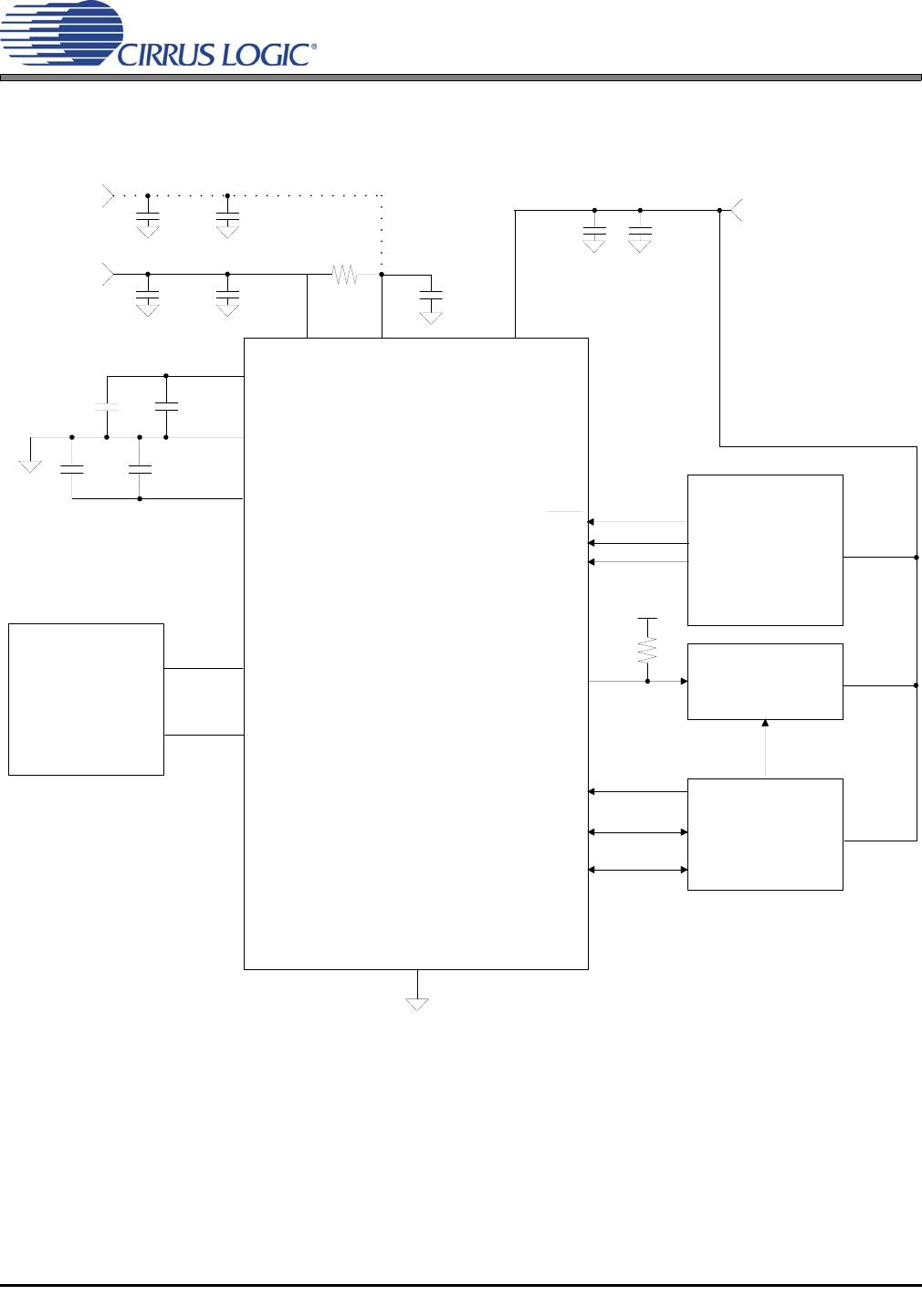
4.2 Operation as Either a Clock Master or Slave
The CS5341 supports operation as either a clock master or slave. As a clock master, the LRCK and SCLK
pins are outputs with the left/right and serial clocks synchronously generated on-chip. As a clock slave, the
LRCK and SCLK pins are inputs and require the left/right and serial clocks to be externally generated. The
selection of clock master or slave is made via the Mode pins as shown in Table 2.
Speed Mode
MCLK/LRCK
Ratio
Output Sample Rate Range (kHz)
Single-Speed Mode
512x 43 - 50
256x 2 - 50
Double-Speed Mode
256x 86 - 100
128x 4 - 100
Quad-Speed Mode
128x 172 - 200
64x* 100 - 200
* Quad-Speed Mode, 64x only available in Master Mode.
M1 (Pin 16) M0 (Pin 1) MODE
00
Clock Master, Single-Speed Mode
01
Clock Master, Double-Speed Mode
10
Clock Master, Quad-Speed Mode
11
Clock Slave, All Speed Modes
Table 2. CS5341 Mode Control

CS5341-DZZR

Mfr. #:
Manufacturer:
Cirrus Logic
Description:
Audio A/D Converter ICs IC 105dB 192 kHz Multi-bit Audio ADC
Lifecycle:
New from this manufacturer.
Delivery:
DHL FedEx Ups TNT EMS
Payment:
T/T Paypal Visa MoneyGram Western Union

Products related to this Datasheet