16 DS564F2
CS5341
Confidential Draft
3/11/08
4.2.1 Operation as a Clock Master
As a clock master, LRCK and SCLK operate as outputs. The left/right and serial clocks are internally de-
rived from the master clock with the left/right clock equal to Fs and the serial clock equal to 64x Fs, as
shown in Figure 18.
4.2.2 Operation as a Clock Slave with Auto-Detect
LRCK and SCLK operate as inputs in clock Slave Mode. It is recommended that the left/right clock be
synchronously derived from the master clock and must be equal to Fs. It is also recommended that the
serial clock be synchronously derived from the master clock and be equal to 64x Fs to maximize system
performance.
A unique feature of the CS5341 is the automatic selection of either Single-, Double- or Quad-Speed Mode
when operating as a clock slave. The auto-mode select feature negates the need to configure the Mode
pins to correspond to the desired mode. The auto-mode selection feature supports all standard audio
sample rates from 2 to 200 kHz. However, there are ranges of non-standard audio sample rates that are
not supported when operating with a fast MCLK (512x, 256x, 128x for Single-, Double-, and Quad-Speed
Modes, respectively). Please refer to Table for supported sample rate ranges.
÷ 128
÷ 256
÷ 64
M0M1
LRCK Output
(Equal to Fs)
Single
Speed
Quad
Speed
Double
Speed
00
01
10
÷ 2
÷ 4
÷ 1
SCLK Output
Single
Speed
Quad
Speed
Double
Speed
00
01
10
÷ 2
÷ 1
0
1
MCLK
Auto-Select
Figure 18. CS5341 Master Mode Clocking
DS564F2 17
CS5341
Confidential Draft
3/11/08
4.2.3 Master Clock
The CS5341 requires a Master clock (MCLK) which runs the internal sampling circuits and digital filters.
There is also an internal MCLK divider which is automatically activated based on the speed mode and
frequency of the MCLK. Table 3 shows a listing of the external MCLK/LRCK ratios that are required.
Table 4 lists some common audio output sample rates and the required MCLK frequency. Please note
that not all of the listed sample rates are supported when operating with a fast MCLK (512x, 256x, 128x
for Single-, Double-, and Quad-Speed Modes, respectively).
4.3 Serial Audio Interface
The CS5341 supports both I²S and Left-Justified serial audio formats. Upon start-up, the CS5341 will detect
the logic level on SDOUT (pin 4). A 10 k pull-up to VL is needed to select I²S format, and a 10 k pull-
down to GND is needed to select Left-Justified format. Figures 19 and 20 illustrate the I²S and Left-Justified
audio formats. Please see Figures 13 through 16, for more information on the required timing for the two
serial audio interface formats. Also see Application Note AN282 for a detailed discussion of the serial audio
interface formats.
Single-Speed Mode Double-Speed Mode Quad-Speed Mode
MCLK/LRCK Ratio 256x, 512x 128x, 256x 64x*,128x
* Quad Speed, 64x only available in Master Mode.
Table 3. Master Clock (MCLK) Ratios
SAMPLE RATE (kHz) MCLK (MHz)
32 8.192
44.1 11.2896
22.5792
48 12.288
24.576
64 8.192
88.2 11.2896
22.5792
96 12.288
24.576
192 12.288
24.576
Table 4. Master Clock (MCLK) Frequencies for Standard Audio Sample Rates
SDATA 23 22 8 7 23 22
SCLK
LRCK
23 226543210 8765432109 9
Left Channel Right Channel
Figure 19. I²S Serial Audio Interface
SDATA 23 22 7 6 23 22
SCLK
LRCK
23 225432108 7654321089 9
Left Channel Right Channel
Figure 20. Left-Justified Serial Audio Interface
18 DS564F2
CS5341
Confidential Draft
3/11/08
4.4 Power-Up Sequence
Reliable power-up can be accomplished by keeping the device in reset until the power supplies, clocks and
configuration pins are stable. It is also recommended that reset be enabled if the analog or digital supplies
drop below the minimum specified operating voltages to prevent power-glitch-related issues.
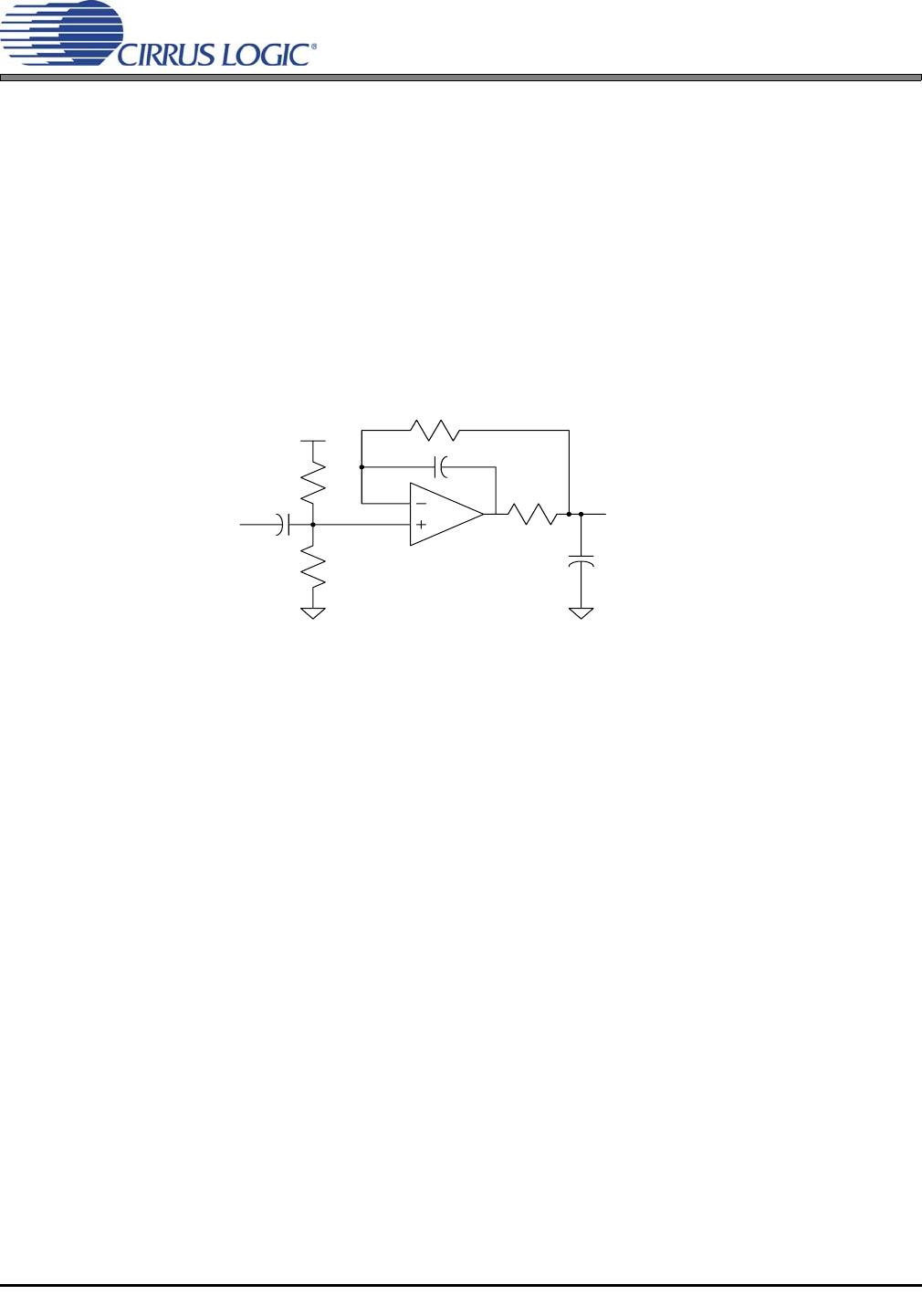
4.5 Analog Connections
The analog modulator samples the input at half of the MCLK frequency, or nominally 6.144 MHz. The digital
filter will reject signals within the stopband of the filter. However, there is no rejection for input signals which
are multiples of the input sampling frequency (n
× 6.144 MHz), where n=0,1,2,... Refer to Figure 21, which
shows the suggested filter that will attenuate any noise energy at 6.144 MHz in addition to providing the op-
timum source impedance for the modulators. The use of capacitors that have a large voltage coefficient
(such as general-purpose ceramics) must be avoided since these can degrade signal linearity.
4.6 Grounding and Power Supply Decoupling
As with any high resolution converter, achieving optimal performance from the CS5341 requires careful at-
tention to power supply and grounding arrangements. Figure 17 shows the recommended power arrange-
ments, with VA and VL connected to clean supplies. VD, which powers the digital filter, may be run from the
system logic supply or may be powered from the analog supply via a resistor. In this case, no additional
devices should be powered from VD. Decoupling capacitors should be as near to the ADC as possible, with
the low-value ceramic capacitor being the nearest. All signals, especially clocks, should be kept away from
the FILT+ and VQ pins in order to avoid unwanted coupling into the modulators. The FILT+ and VQ decou-
pling capacitors, particularly the 0.01 µF, must be positioned to minimize the electrical path from FILT+ and
REF_GND. Furthermore, all ground pins on CS5341 should be referenced to the same ground reference.
The CDB5341 evaluation board demonstrates the optimum layout and power supply arrangements. To min-
imize digital noise, connect the ADC digital outputs only to CMOS inputs.
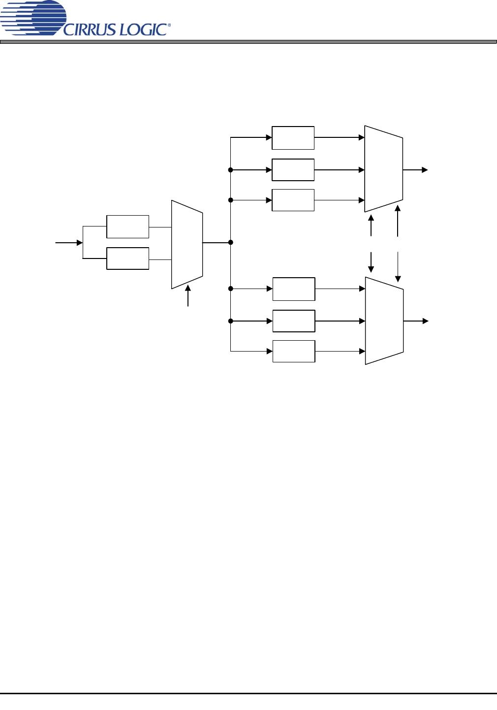
4.7 Synchronization of Multiple Devices
In systems where multiple ADCs are required, the user can achieve simultaneous sampling if the MCLK and
LRCK signals are the same for all of the CS5341’s in the system. If only one master clock source is needed,
one solution is to place one CS5341 in Master Mode, and slave all of the other CS5341’s to the one master.
If multiple master clock sources are needed, a possible solution would be to supply all clocks from the same
external source and time the CS5341 reset with the inactive (falling) edge of MCLK. This will ensure that all
converters begin sampling on the same clock edge.
VA
4.7 µF
470 pF
C0G
2700 pF
CS5341 AINx
AINx
100 k
100 k
634
91
Figure 21. CS5341 Recommended Analog Input Buffer

CS5341-DZZR

Mfr. #:
Manufacturer:
Cirrus Logic
Description:
Audio A/D Converter ICs IC 105dB 192 kHz Multi-bit Audio ADC
Lifecycle:
New from this manufacturer.
Delivery:
DHL FedEx Ups TNT EMS
Payment:
T/T Paypal Visa MoneyGram Western Union

Products related to this Datasheet