Electrical specifications L9954 / L9954XP
10/37 Doc ID 14279 Rev 4
2.4 Electrical characteristics
V
S
= 8 to 16V, V
CC
= 4.5 to 5.3V, T
j
= - 40 to 150°C, unless otherwise specified. The
voltages are referred to GND and currents are assumed positive, when the current flows
into the pin.
Table 6. Temperature warning and thermal shutdown
Symbol Parameter Min. Typ. Max. Unit
T
jTW ON
Temperature warning threshold junction
temperature
T
j
130 150 °C
T
jSD ON
Thermal shutdown threshold junction
temperature
T
j
increasing
170 °C
T
jSD OFF
Thermal shutdown threshold junction
temperature
T
j
decreasing
150 °C
T
jSD HYS
Thermal shutdown hysteresis 5 °K
Table 7. Supply
Symbol Parameter Test condition Min. Typ. Max Unit
V
S
Operating supply voltage
range
728V
I
S
V
S
DC supply current
V
S
= 16V, V
CC
= 5.3V
active mode
OUT1 - OUT6 floating
720mA
V
S
quiescent supply current
V
S
= 16V, V
CC
= 0V
standby mode
OUT1 - OUT6 floating
T
test
= -40°C, 25°C
412µA
T
test
= 85°C
(1)
1. Guaranteed by design.
625µA
I
CC
V
CC
DC supply current
V
S
= 16V, V
CC
= 5.3V
CSN = V
CC ,
active mode
13mA
V
CC
quiescent supply
current
V
S
= 16V, V
CC
= 5.3V
CSN = V
CC
standby mode
OUT1 - OUT6 floating
25 50 µA
I
S
+ I
CC
Sum quiescent supply
current
V
S
= 16V, V
CC
= 5.3V
CSN = V
CC
standby mode
OUT1 - OUT6 floating
T
test
= 130°C
50 100 µA
L9954 / L9954XP Electrical specifications
Doc ID 14279 Rev 4 11/37
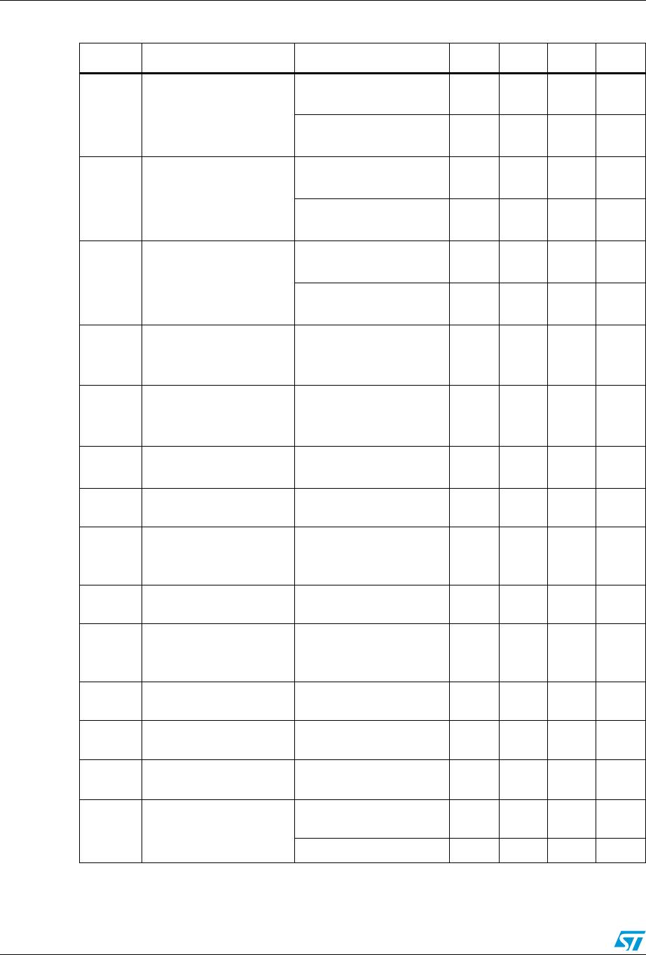
Table 8. Overvoltage and undervoltage detection
Symbol Parameter Test condition Min. Typ. Max Unit
V
SUV ON
VS UV-threshold voltage V
S
increasing 5.7 7.2 V
V
SUV OFF
VS UV-threshold voltage V
S
decreasing 5.5 6.9 V
V
SUV hyst
VS UV-hysteresis V
SUV ON
- V
SUV OFF
0.5 V
V
SOV OFF
VS OV-threshold voltage V
S
increasing 18 24.5 V
V
SOV ON
VS OV-threshold voltage V
S
decreasing 17.5 23.5 V
V
SOV hyst
VS OV-hysteresis V
SOV OFF
- V
SOV ON
1V
V
POR OFF
Power-On-reset threshold V
CC
increasing 4.4 V
V
POR ON
Power-On-reset threshold V
CC
decreasing 3.1 V
V
POR hyst
Power-On-reset hysteresis V
POR OFF
- V
POR ON
0.3 V
Table 9. Current monitor output
Symbol Parameter Test condition Min. Typ. Max. Unit
V
CM
Functional voltage range V
CC
= 5V 0 4 V
I
CM,r
Current monitor output
ratio:
I
CM
/I
OUT1,4,5,6
0V V
CM
4V, VCC=5V -
I
CM acc
Current monitor accuracy
0 V V
CM
3.8V,
V
CC
= 5V, I
Out,min
=500mA,
I
Out max
= 6A
(FS = full scale= 600μA)
4% +
1%FS
8% +
2%FS
-
Table 10. Charge pump output
Symbol Parameter Test condition Min. Typ. Max. Unit
V
CP
Charge pump output
voltage
V
S
= 8V, I
CP
= -60μAV
S
+6 V
S
+13 V
V
S
= 10V, I
CP
= -80μAV
S
+8 V
S
+13 V
V
S
12V, I
CP
= -100μAV
S
+10 V
S
+13 V
I
CP
Charge pump output
current
V
CP
= V
S
+10V, V
S
=13.5V 95 150 300 µA
1
10.000
------------------
Electrical specifications L9954 / L9954XP
12/37 Doc ID 14279 Rev 4
Table 11. OUT1 - OUT6
Symbol Parameter Test condition Min. Typ. Max. Unit
r
ON OUT1,
r
ON OUT2
r
ON OUT3
On-resistance to supply
or GND
V
S
= 13.5 V, T
j
= 25 °C,
I
OUT1,2,3
= ± 0.8A
800 1100 mΩ
V
S
= 13.5 V, T
j
= 125 °C,
I
OUT1,2,3
= ± 0.8 A
1250 1700 mΩ
r
ON OUT4,
r
ON OUT5
On-resistance to supply
V
S
= 13.5 V, T
j
= 25 °C,
I
OUT4,5
= −0.8 A
500 700 mΩ
V
S
= 13.5 V, T
j
= 125 °C,
I
OUT4,5
= −0.8 A
700 950 mΩ
r
ON OUT6
On-resistance to supply
VS = 13.5 V, T
j
= 25 °C,
I
OUT6
= 3 A
100 150 mΩ
V
S
= 13.5 V, T
j
= 125 °C,
I
OUT6
= −3 A
150 200 mΩ
I
OUT1
I
OUT2
I
OUT3
Output current limitation
to GND
Source, V
S
=13.5 V -3.0 -1.5 A
I
OUT1
I
OUT2
I
OUT3
Output current limitation
to supply
Sink, V
S
=13.5 V 1.5 3.0 A
I
OUT4
I
OUT5
Output current limitation
to GND
Source, V
S
=13.5 V -3.0 -1.5 A
I
OUT6
Output current limitation
to GND
Source, V
S
=13.5 V -10.5 -6 A
t
d ON H
Output delay time,
highside driver On
V
S
=13.5 V,
corresponding lowside
driver is not active
20 40 80 µs
t
d OFF H
Output delay time,
highside driver Off
V
S
=13.5 V 50 150 300 µs
t
d ON L
Output delay time,
lowside driver On
V
S
=13.5 V,
corresponding highside
driver is not active
15 30 70 µs
t
d OFF L
Output delay time,
lowside driver Off
V
S
=13.5 V 80 150 300 µs
t
d HL
Cross current protection
time, source to sink
t
CC ONLS_OFFHS
- t
d
OFF H
(1)
200 400 µs
t
d LH
Cross current protection
time, sink to source
t
CC ONHS_OFFLS
- t
d
OFF L
(1)
200 400 µs
I
QLH
Switched-off output
current highside drivers of
OUT1-6
V
OUT1-6
= 0V, standby
mode
0-2-5µA
V
OUT1-6
= 0V, active mode -40 -15 0 µA

L9954

Mfr. #:
Manufacturer:
STMicroelectronics
Description:
IC DVR DOOR ACTUATOR POWERSO-36
Lifecycle:
New from this manufacturer.
Delivery:
DHL FedEx Ups TNT EMS
Payment:
T/T Paypal Visa MoneyGram Western Union

Products related to this Datasheet