Application information L9954 / L9954XP
22/37 Doc ID 14279 Rev 4
3.13 Programmable softstart function to drive loads with higher
inrush current
Loads with start-up currents higher than the over-current limits (e.g. inrush current of lamps,
start current of motors and cold resistance of heaters) can be driven by using the
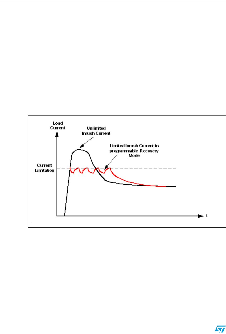
programmable softstart function (i.e. overcurrent recovery mode). Each driver has a
corresponding over-current recovery bit. If this bit is set, the device will automatically switch-
on the outputs again after a programmable recovery time. The duty cycle in over-current
condition can be programmed by the SPI interface to be about 15% ...25%. The PWM
modulated current will provide sufficient average current to power up the load (e.g. heat up
the bulb) until the load reaches operating condition. The PWM frequency settles at 1.5 kHz
or 3 kHz. The device itself cannot distinguish between a real overload and a non linear load
like a light bulb. A real overload condition can only be qualified by time. As an example the
microcontroller can switch on light bulbs by setting the over-current recovery bit for the first
50ms. After clearing the recovery bit the output will be automatically disabled if the overload
condition still exits.
Figure 9. Example of programmable softstart function for inductive loads
L9954 / L9954XP Functional description of the SPI
Doc ID 14279 Rev 4 23/37
4 Functional description of the SPI
4.1 Serial Peripheral Interface (SPI)
This device uses a standard SPI to communicate with a microcontroller. The SPI can be
driven by a microcontroller with its SPI peripheral running in following mode: CPOL = 0 and
CPHA = 0.
For this mode, input data is sampled by the low to high transition of the clock CLK, and
output data is changed from the high to low transition of CLK.
This device is not limited to microcontroller with a build-in SPI. Only three CMOS-compatible
output pins and one input pin will be needed to communicate with the device. A fault
condition can be detected by setting CSN to low. If CSN = 0, the DO-pin will reflect the
status bit 0 (fault condition) of the device which is a logical-or of all bits in the status registers
0 and 1. The microcontroller can poll the status of the device without the need of a full SPI-
communication cycle.
Note: In contrast to the SPI-standard the least significant bit (LSB) will be transferred first
(see Figure 3).
4.2 Chip Select Not (CSN)
The input pin is used to select the serial interface of this device. When CSN is high, the
output pin (DO) will be in high impedance state. A low signal will activate the output driver
and a serial communication can be started. The state when CSN is going low until the rising
edge of CSN will be called a communication frame. If the CSN-input pin is driven above
7.5V, the L9954 will go into a test mode. In the test mode the DO will go from tri-state to
active mode.
4.3 Serial Data In (DI)
The input pin is used to transfer data serial into the device. The data applied to the DI will be
sampled at the rising edge of the CLK signal and shifted into an internal 24 bit shift register.
At the rising edge of the CSN signal the contents of the shift register will be transferred to
Data Input Register. The writing to the selected Data Input Register is only enabled if exactly
24 bits are transmitted within one communication frame (i.e. CSN low). If more or less clock
pulses are counted within one frame the complete frame will be ignored. This safety function
is implemented to avoid an activation of the output stages by a wrong communication frame.
Note: Due to this safety functionality a daisy chaining of SPI is not possible. Instead, a parallel
operation of the SPI bus by controlling the CSN signal of the connected ICs is
recommended.
4.4 Serial Data Out (DO)
The data output driver is activated by a logical low level at the CSN input and will go from
high impedance to a low or high level depending on the status bit 0 (fault condition). The first
rising edge of the CLK input after a high to low transition of the CSN pin will transfer the
Functional description of the SPI L9954 / L9954XP
24/37 Doc ID 14279 Rev 4
content of the selected status register into the data out shift register. Each subsequent
falling edge of the CLK will shift the next bit out.
4.5 Serial clock (CLK)
The CLK input is used to synchronize the input and output serial bit streams. The data input
(DI) is sampled at the rising edge of the CLK and the data output (DO) will change with the
falling edge of the CLK signal.
4.6 Input data register
The device has two input registers. The first bit (bit 0) at the DI-input is used to select one of
the two Input Registers. All bits are first shifted into an input shift register. After the rising
edge of CSN the contents of the input shift register will be written to the selected Input Data
Register only if a frame of exact 24 data bits are detected. Depending on bit 0 the contents
of the selected status register will be transferred to DO during the current communication
frame. Bit 1-17 controls the behavior of the corresponding driver.
If bit 23 is zero, the device will go into the standby-mode. The bits 18 and 19 are used to
control the current monitor multiplexer. Bit 22 is used to reset all status bits in both status
registers. The bits in the status registers will be cleared after the current communication
frame (rising edge of CSN).
4.7 Status register
This devices uses two status registers to store and to monitor the state of the device. No
error bit (bit 0) is used as a fault bit and is a logical-NOR combination of bits 1-22 in both
status registers. The state of this bit can be polled by the microcontroller without the need of
a full SPI-communication cycle. If one of the over-current bits is set, the corresponding
driver will be disabled. If the over-current recovery bit of the output is not set the
microcontroller has to clear the over-current bit to enable the driver. If the thermal shutdown
bit is set, all drivers will go into a high impedance state. Again the microcontroller has to
clear the bit to enable the drivers.

L9954

Mfr. #:
Manufacturer:
STMicroelectronics
Description:
IC DVR DOOR ACTUATOR POWERSO-36
Lifecycle:
New from this manufacturer.
Delivery:
DHL FedEx Ups TNT EMS
Payment:
T/T Paypal Visa MoneyGram Western Union

Products related to this Datasheet