Electrical specifications L9954 / L9954XP
14/37 Doc ID 14279 Rev 4
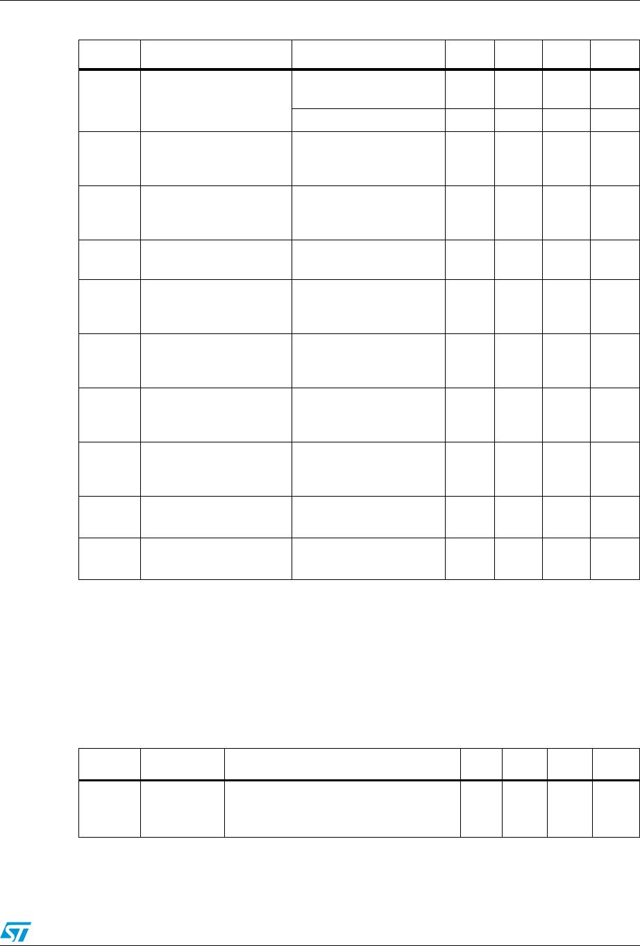
Table 13. Inputs: CSN, CLK, PWM1/2 and DI
Symbol Parameter Test condition Min. Typ. Max. Unit
V
inL
Input low level V
CC
= 5V 1.5 2.0 V
V
inH
Input high level V
CC
= 5V 3.0 3.5 V
V
inHyst
Input hysteresis V
CC
= 5V 0.5 V
I
CSN in
Pull up current at input CSN V
CSN
= 3.5V V
CC
= 5V -40 -20 -5 µA
I
CLK in
Pull down current at input CLK V
CLK
= 1.5V 10 25 50 µA
I
DI in
Pull down current at input DI V
DI
= 1.5V 10 25 50 µA
I
PWM1 in
Pull down current at input
PWM1
V
PWM
= 1.5V 10 25 50 µA
C
in
(1)
1. Value of input capacity is not measured in production test. Parameter guaranteed by design.
Input capacitance at input
CSN, CLK, DI and PWM1/2
0 V < V
CC
< 5.3V 10 15 pF
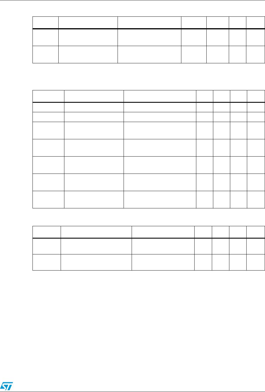
Table 14. DI timing
(1)
1. DI timing parameters tested in production by a passed / failed test:
Tj= -40°C / +25°C: SPI communication @ 2MHz.
Tj= +125°C SPI communication @ 1.25 MHz.
Symbol Parameter Test condition Min. Typ. Max. Unit
t
CLK
Clock period V
CC
= 5V 1000 ns
t
CLKH
Clock high time V
CC
= 5V 400 ns
t
CLKL
Clock low time V
CC
= 5V 400 ns
t
set CSN
CSN setup time, CSN low
before rising edge of CLK
V
CC
= 5V 400 ns
t
set CLK
CLK setup time, CLK high
before rising edge of CSN
V
CC
= 5V 400 ns
t
set DI
DI setup time V
CC
= 5V 200 ns
t
hold DI
DI hold time V
CC
= 5V 200 ns
t
r in
Rise time of input signal DI,
CLK, CSN
V
CC
= 5V 100 ns
t
f in
Fall time of input signal DI,
CLK, CSN
V
CC
= 5V 100 ns
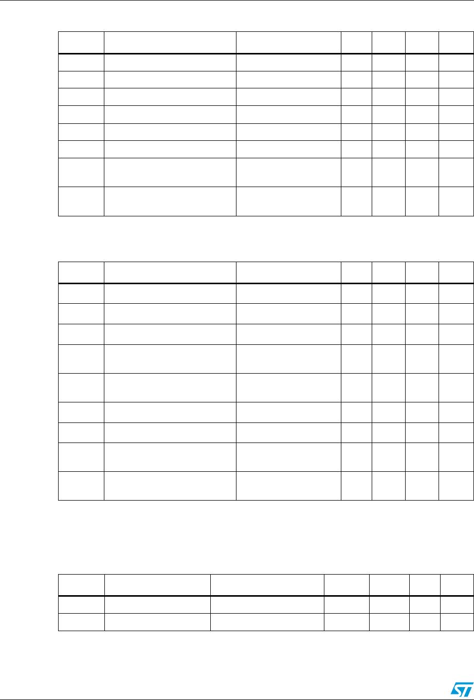
Table 15. DO
Symbol Parameter Test condition Min. Typ. Max. Unit
V
DOL
Output low level VCC = 5 V, I
D
= -2mA 0.2 0.4 V
V
DOH
Output high level VCC = 5 V, I
D
= 2 mA V
CC
-0.4 V
CC
-0.2 V