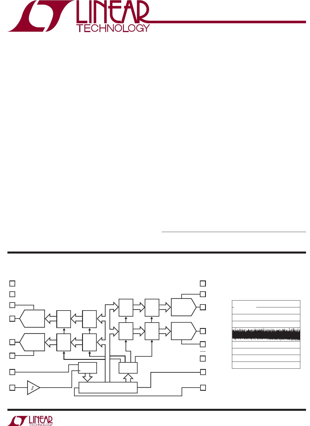
LTC2604/LTC2614/LTC2624
2
2604fd
1
2
3
4
5
6
7
8
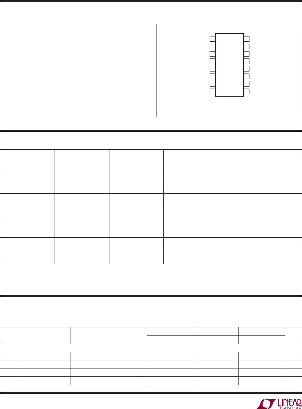
TOP VIEW
GN PACKAGE
16-LEAD PLASTIC SSOP
16
15
14
13
12
11
10
9
GND
REF LO
REF A
V
OUT A
V
OUT B
REF B
CS/LD
SCK
V
CC
REF D
V
OUT D
V
OUT C
REF C
CLR
SDO
SDI
T
JMAX
= 125°C, θ
JA
= 150°C/W
ABSOLUTE MAXIMUM RATINGS PIN CONFIGURATION
ORDER INFORMATION
The ● denotes specifi cations which apply over the full operating
temperature range, otherwise specifi cations are at T
A
= 25°C. REF A = REF B = REF C = REF D = 4.096V (V
CC
= 5V), REF A = REF B =
REF C = REF D = 2.048V (V
CC
= 2.5V), REF LO = 0V, V
OUT
unloaded, unless otherwise noted. (Note 10)
LEAD FREE FINISH TAPE AND REEL PART MARKING PACKAGE DESCRIPTION TEMPERATURE RANGE
LTC2604CGN#PBF LTC2604CGN#TRPBF 2604
16-Lead Narrow SSOP Package
0°C to 70°C
LTC2604CGN-1#PBF LTC2604CGN-1#TRPBF 26041
16-Lead Narrow SSOP Package
0°C to 70°C
LTC2604IGN#PBF LTC2604IGN#TRPBF 2604I
16-Lead Narrow SSOP Package
–40°C to 85°C
LTC2604IGN-1#PBF LTC2604IGN-1#TRPBF 2604I1
16-Lead Narrow SSOP Package
–40°C to 85°C
LTC2614CGN#PBF LTC2614CGN#TRPBF 2614
16-Lead Narrow SSOP Package
0°C to 70°C
LTC2614CGN-1#PBF LTC2614CGN-1#TRPBF 26141
16-Lead Narrow SSOP Package
0°C to 70°C
LTC2614IGN#PBF LTC2614IGN#TRPBF 2614I
16-Lead Narrow SSOP Package
–40°C to 85°C
LTC2614IGN-1#PBF LTC2614IGN-1#TRPBF 2614I1
16-Lead Narrow SSOP Package
–40°C to 85°C
LTC2624CGN#PBF LTC2624CGN#TRPBF 2624
16-Lead Narrow SSOP Package
0°C to 70°C
LTC2624CGN-1#PBF LTC2624CGN-1#TRPBF 26241
16-Lead Narrow SSOP Package
0°C to 70°C
LTC2624IGN#PBF LTC2624IGN#TRPBF 2624I
16-Lead Narrow SSOP Package
–40°C to 85°C
LTC2624IGN-1#PBF LTC2624IGN-1#TRPBF 2624I1
16-Lead Narrow SSOP Package
–40°C to 85°C
Consult LTC Marketing for parts specifi ed with wider operating temperature ranges.
Consult LTC Marketing for information on non-standard lead based fi nish parts.
For more information on lead free part marking, go to:
http://www.linear.com/leadfree/
For more information on tape and reel specifi cations, go to:
http://www.linear.com/tapeandreel/
ELECTRICAL CHARACTERISTICS
SYMBOL PARAMETER CONDITIONS
LTC2624/LTC2624-1 LTC2614/LTC2614-1 LTC2604/LTC2604-1
UNITSMIN TYP MAX MIN TYP MAX MIN TYP MAX
DC Performance
Resolution
l
12 14 16 Bits
Monotonicity (Note 2)
l
12 14 16 Bits
DNL Differential Nonlinearity (Note 2)
l
±0.5 ±1 ±1 LSB
INL Integral Nonlinearity (Note 2)
l
±0.9 ±4 ±4 ±16 ±14 ±64 LSB
Any Pin to GND ............................................ –0.3V to 6V
Any Pin to V
CC
............................................. –6V to 0.3V
Maximum Junction Temperature .......................... 125°C
Operating Temperature Range
LTC2604C/LTC2614C/LTC2624C ............. 0°C to 70°C
LTC2604C-1/LTC2614C-1/
LTC2624C-1 ............................................. 0°C to 70°C
LTC2604I/LTC2614I/LTC2624I .............–40°C to 85°C
LTC2604I-1/LTC2614I-1/
LTC2624I-1 ..........................................–40°C to 85°C
Storage Temperature Range ..................–65°C to 150°C
Lead Temperature (Soldering, 10 sec)...................300°C
(Note 1)