LTC2604/LTC2614/LTC2624
12
2604fd
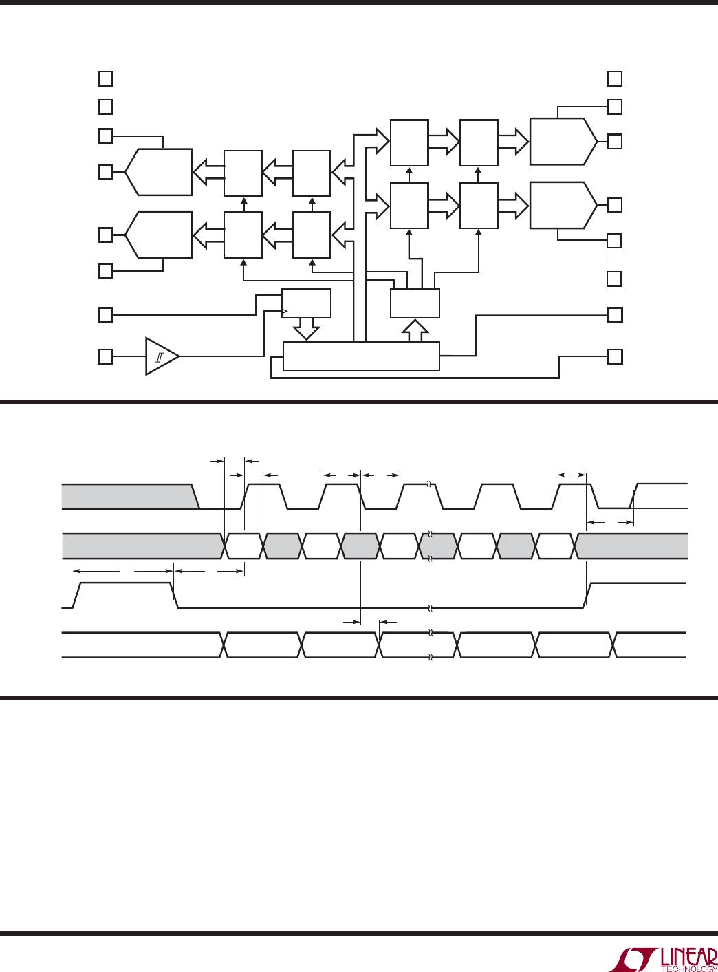
OPERATION
operation copies the data word from the input register to
the DAC register. Once copied into the DAC register, the
data word becomes the active 16-, 14- or 12-bit input
code, and is converted to an analog voltage at the DAC
output. The update operation also powers up the selected
DAC if it had been in power-down mode. The data path
and registers are shown in the block diagram.
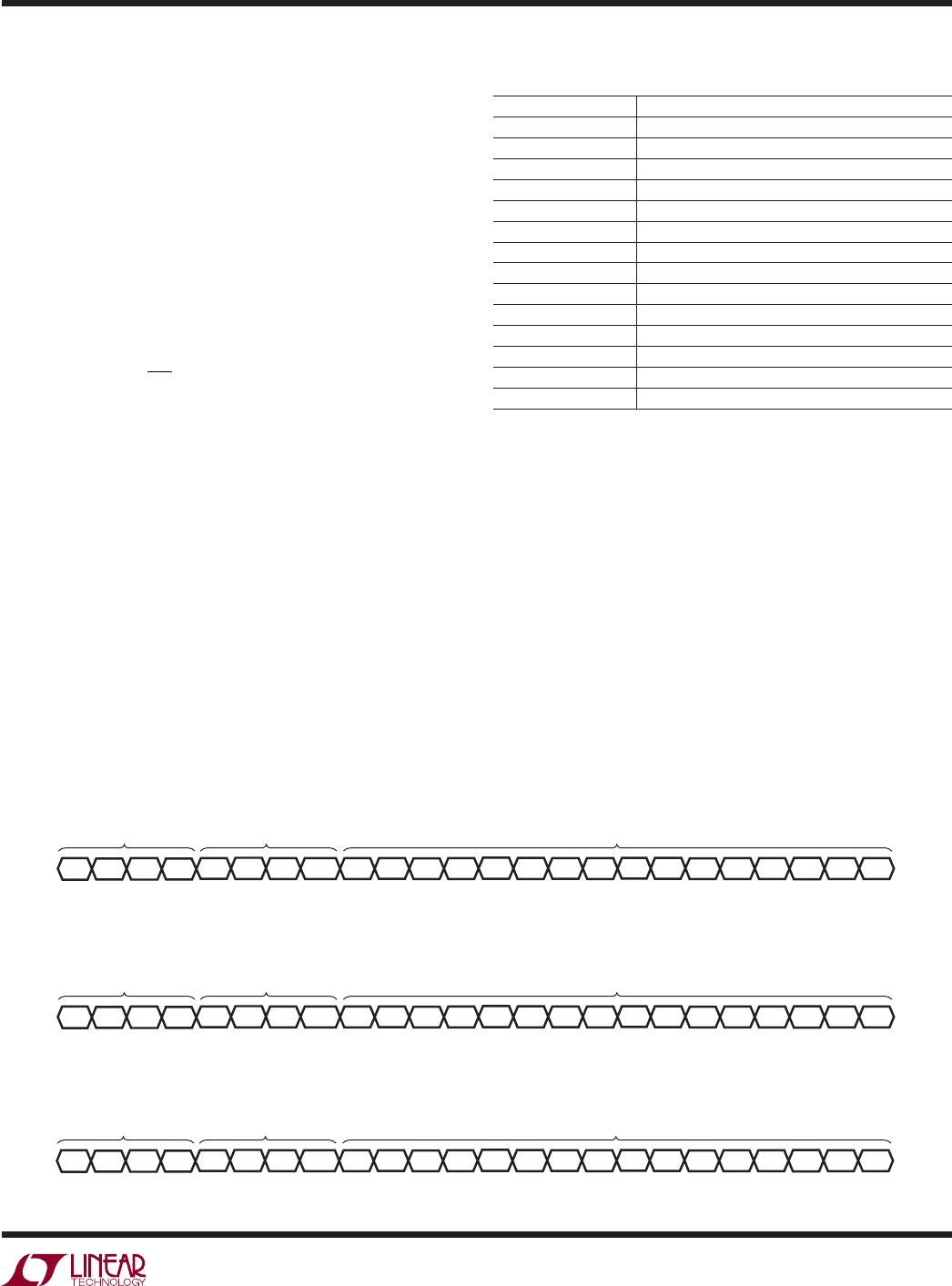
While the minimum input word is 24 bits, it may optionally
be extended to 32 bits. To use the 32-bit word width, 8
don’t-care bits are transferred to the device fi rst, followed
by the 24-bit word as just described. Figure 2b shows the
32-bit sequence. The 32-bit word is required for daisy-
chain operation, and is also available to accommodate
microprocessors which have a minimum word width of
16 bits (2 bytes).
Daisy-Chain Operation
The serial output of the shift register appears at the SDO
pin. Data transferred to the device from the SDI input is
delayed 32 SCK rising edges before being output at the
next SCK falling edge.
The SDO output can be used to facilitate control of multiple
serial devices from a single 3-wire serial port (i.e., SCK,
SDI and CS/LD). Such a “daisy-chain” series is confi gured
by connecting SDO of each upstream device to SDI of the
next device in the chain. The shift registers of the devices
are thus connected in series, effectively forming a single
input shift register which extends through the entire
chain. Because of this, the devices can be addressed and
controlled individually by simply concatenating their input
words; the fi rst instruction addresses the last device in
the chain and so forth. The SCK and CS/LD signals are
common to all devices in the series.
In use, CS/LD is fi rst taken low. Then the concatenated
input data is transferred to the chain, using SDI of the
fi rst device as the data input. When the data transfer is
complete, CS/LD is taken high, completing the instruction
sequence for all devices simultaneously. A single device
can be controlled by using the no-operation command
(1111) for the other devices in the chain.
Power-Down Mode
For power-constrained applications, power-down mode can
be used to reduce the supply current whenever less than
four outputs are needed. When in power-down, the buffer
amplifi ers, bias circuits and reference inputs are disabled,
and draw essentially zero current. The DAC outputs are
put into a high-impedance state, and the output pins are
passively pulled to ground through individual 90k resis-
tors. Input- and DAC-register contents are not disturbed
during power-down.
Any channel or combination of channels can be put into
power-down mode by using command 0100
b
in combi-
nation with the appropriate DAC address, (n). The 16-bit
data word is ignored. The supply current is reduced by
approximately 1/4 for each DAC powered down. The ef-
fective resistance at REF x (pins 3, 6, 12 and 15) are at
high-impedance input (typically > 1GΩ) when the cor-
responding DACs are powered down.
Normal operation can be resumed by executing any com-
mand which includes a DAC update, as shown in Table 1.
The selected DAC is powered up as its voltage output is
updated. When a DAC which is in a powered-down state
is powered up and updated, normal settling is delayed. If
less than four DACs are in a powered-down state prior to
the update command, the power-up delay time is 5μs. If on
the other hand, all four DACs are powered down, then the
main bias generation circuit block has been automatically
shut down in addition to the individual DAC amplifi ers and
reference inputs. In this case, the power up delay time is
12μs (for V
CC
= 5V) or 30μs (for V
CC
= 3V).
Voltage Outputs
Each of the four rail-to-rail amplifi ers contained in these
parts has guaranteed load regulation when sourcing or
sinking up to 15mA at 5V (7.5mA at 3V).
Load regulation is a measure of the amplifi er’s ability to
maintain the rated voltage accuracy over a wide range of
load conditions. The measured change in output voltage
per milliampere of forced load current change is expressed
in LSB/mA.