LTC2604/LTC2614/LTC2624
9
2604fd
PIN FUNCTIONS
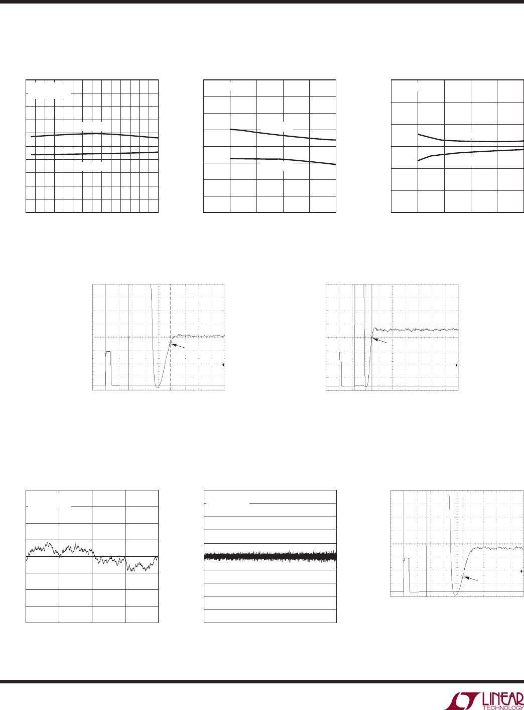
2μs/DIV
2604 G33
V
OUT
1mV/DIV
CS/LD
2V/DIV
V
CC
= 5V, V
REF
= 4.096V
1/4-SCALE TO 3/4-SCALE STEP
R
L
= 2k, C
L
= 200pF
AVERAGE OF 2048 EVENTS
6.8μs
CODE
0 1024 2048 3072 4095
DNL (LSB)
2604 G32
V
CC
= 5V
V
REF
= 4.096V
1.0
0.8
0.6
0.4
0.2
0
–0.2
–0.4
–0.6
–0.8
–1.0
CODE
0
1024 2048 3072 4095
INL (LSB)
2604 G31
2.0
1.5
1.0
0.5
0
–0.5
–1.0
–1.5
–2.0
V
CC
= 5V
V
REF
= 4.096V
Differential Nonlinearity (DNL) Settling to ±1LSB
(LTC2624/LTC2624-1)
Integral Nonlinearity (INL)
GND (Pin 1): Analog Ground.
REF LO (Pin 2): Reference Low. The voltage at this pin
sets the zero scale (ZS) voltage of all DACs. This pin can
be raised up to 1V above ground at V
CC
= 5V or 100mV
above ground at V
CC
= 3V.
REF A, REF B, REF C, REF D (Pins 3, 6, 12, 15): Refer-
ence Voltage Inputs for each DAC. REF x sets the full scale
voltage of the DACs. 0V ≤ REF x ≤ V
CC
.
V
OUT A
to V
OUT D
(Pins 4, 5, 13, 14): DAC Analog Voltage
Outputs. The output range is from REF LO to REF x.
CS/LD (Pin 7): Serial Interface Chip Select/Load Input. When
CS/LD is low, SCK is enabled for shifting data on SDI into
the register. When CS/LD is taken high, SCK is disabled
and the specifi ed command (see Table 1) is executed.
SCK (Pin 8): Serial Interface Clock Input. CMOS and TTL
compatible.
SDI (Pin 9): Serial Interface Data Input. Data is applied to
SDI for transfer to the device at the rising edge of SCK.
The LTC2604/LTC2604-1, LTC2614/LTC2614-1, LTC2624/
LTC2624-1 accept input word lengths of either 24 or
32 bits.
SDO (Pin 10): Serial Interface Data Output. This pin is
used for daisy-chain operation. The serial output of the
shift register appears at the SDO pin. The data transferred
to the device via the SDI pin is delayed 32 SCK rising
edges before being output at the next falling edge. SDO
is an active output and does not go high impedance, even
when CS/LD is taken to a logic high level.
CLR (Pin 11): Asynchronous Clear Input. A logic low at
this level-triggered input clears all registers and causes
the DAC voltage outputs to drop to 0V for the LTC2604/
LTC2614/LTC2624. A logic low at this input sets all registers
to midscale code and causes the DAC voltage outputs to
go to midscale for the LTC2604-1/LTC2614-1/LTC2624-1.
CMOS and TTL compatible.
V
CC
(Pin 16): Supply Voltage Input. 2.5V ≤ V
CC
≤ 5.5V.
TYPICAL PERFORMANCE CHARATERISTICS