LTC2604/LTC2614/LTC2624
4
2604fd
The denotes specifi cations which apply over the full operating
temperature range, otherwise specifi cations are at T
A
= 25°C. REF A = REF B = REF C = REF D = 4.096V (V
CC
= 5V), REF A = REF B =
REF C = REF D = 2.048V (V
CC
= 2.5V), REF LO = 0V, V
OUT
unloaded, unless otherwise noted. (Note 10)
ELECTRICAL CHARACTERISTICS
SYMBOL PARAMETER CONDITIONS
LTC2624/LTC2624-1 LTC2614/LTC2614-1 LTC2604/LTC2604-1
MIN TYP MAX MIN TYP MAX MIN TYP MAX UNITS
AC Performance
t
s
Settling Time (Note 8) ±0.024% (±1LSB at 12 Bits)
±0.006% (±1LSB at 14 Bits)
±0.0015% (±1LSB at 16 Bits)
77
9
7
9
10
μs
μs
μs
Settling Time for
1LSB Step (Note 9)
±0.024% (±1LSB at 12 Bits)
±0.006% (±1LSB at 14 Bits)
±0.0015% (±1LSB at 16 Bits)
2.7 2.7
4.8
2.7
4.8
5.2
μs
μs
μs
Voltage Output Slew Rate 0.80 0.80 0.80 V/μs
Capacitive Load Driving 1000 1000 1000 pF
Glitch Impulse At Midscale Transition 12 12 12 nV • s
Multiplying Bandwidth 180 180 180 kHz
e
n
Output Voltage Noise
Density
At f = 1kHz
At f = 10kHz
120
100
120
100
120
100
nV√Hz
nV√Hz
Output Voltage Noise 0.1Hz to 10Hz
15 15 15 μV
P–P
SYMBOL PARAMETER CONDITIONS MIN TYP MAX UNITS
V
CC
= 2.5V to 5.5V
t
1
SDI Valid to SCK Setup
l
4ns
t
2
SDI Valid to SCK Hold
l
4ns
t
3
SCK High Time
l
9ns
t
4
SCK Low Time
l
9ns
t
5
CS/LD Pulse Width
l
10 ns
t
6
LSB SCK High to CS/LD High
l
7ns
t
7
CS/LD Low to SCK High
l
7ns
t
8
SDO Propagation Delay from SCK Falling Edge C
LOAD
= 10pF
V
CC
= 4.5V to 5.5V
V
CC
= 2.5V to 5.5V
l
l
20
45
ns
ns
t
9
CLR Pulse Width
l
20 ns
SYMBOL PARAMETER CONDITIONS MIN TYP MAX UNITS
V
IL
Digital Input Low Voltage V
CC
= 4.5V to 5.5V
V
CC
= 2.5V to 5.5V
l
l
0.8
0.6
V
V
V
OH
Digital Output High Voltage Load Current = –100μA
l
V
CC
– 0.4 V
V
OL
Digital Output Low Voltage Load Current = +100μA
l
0.4 V
I
LK
Digital Input Leakage V
IN
= GND to V
CC
l
±1 μA
C
IN
Digital Input Capacitance (Note 6)
l
8pF
The denotes specifi cations which apply over the full operating temperature
range, otherwise specifi cations are at T
A
= 25°C. REF A = REF B = REF C = REF D = 4.096V (V
CC
= 5V), REF A = REF B = REF C = REF D
= 2.048V (V
CC
= 2.5V), REF LO = 0V, V
OUT
unloaded, unless otherwise noted. (Note 10)
TIMING CHARACTERISTICS
The denotes specifi cations which apply over the full operating temperature range, otherwise specifi cations are at T
A
= 25°C. REF
A = REF B = REF C = REF D = 4.096V (V
CC
= 5V), REF A = REF B = REF C = REF D = 2.048V (V
CC
= 2.5V), REF LO = 0V, V
OUT
unloaded,
unless otherwise noted. (Note 10)
LTC2604/LTC2614/LTC2624
5
2604fd
TYPICAL PERFORMANCE CHARACTERISTICS
Note 1: Stresses beyond those listed under Absolute Maximum Ratings
may cause permanent damage to the device. Exposure to any Absolute
Maximum Rating condition for extended periods may affect device
reliability and lifetime.
Note 2: Linearity and monotonicity are defi ned from code k
L
to code
2
N
– 1, where N is the resolution and k
L
is given by k
L
= 0.016(2
N
/V
REF
),
rounded to the nearest whole code. For V
REF
= 4.096V and N = 16,
k
L
= 256, linearity is defi ned from code 256 to code 65,535.
Note 3: Digital inputs at 0V or V
CC
.
Note 4: DC crosstalk is measured with V
CC
= 5V and V
REF
= 4.096V, with
the measured DAC at midscale, unless otherwise noted.
Note 5: R
L
= 2kΩ to GND or V
CC
.
Note 6: Guaranteed by design and not production tested.
Note 7: Inferred from measurement at code 256 (LTC2604), code 64
(LTC2614) or code 16 (LTC2624), and at full scale.
Note 8: V
CC
= 5V, V
REF
= 4.096V. DAC is stepped 1/4 scale to 3/4 scale and
3/4 scale to 1/4 scale. Load is 2k in parallel with 200pF to GND.
Note 9: V
CC
= 5V, V
REF
= 4.096V. DAC is stepped 1LSB between half scale
and half scale –1. Load is 2k in parallel with 200pF to GND.
Note 10: These specifi cations apply to LTC2604/LTC2604-1, LTC2614/
LTC2614-1, LTC2624/LTC2624-1.
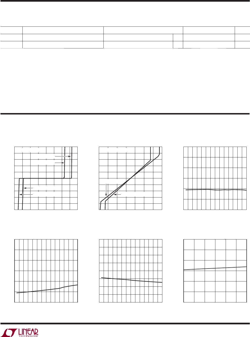
TEMPERATURE (°C)
–50 –30 –10 10 30 50 70 90
OFFSET ERROR (mV)
2604 G03
3
2
1
0
–1
–2
–3
I
OUT
(mA)
–35 –25 –15 –5 5 15 25 35
ΔV
OUT
(mV)
2604 G02
1.0
0.8
0.6
0.4
0.2
0
–0.2
–0.4
–0.6
–0.8
–1.0
V
REF
= V
CC
= 5V
CODE = MIDSCALE
V
REF
= V
CC
= 3V
I
OUT
(mA)
–40 –30 –20 –10 0 10 20 30 40
ΔV
OUT
(V)
2604 G01
0.10
0.08
0.06
0.04
0.02
0
–0.02
–0.04
–0.06
–0.08
–0.10
V
REF
= V
CC
= 5V
V
REF
= V
CC
= 3V
V
REF
= V
CC
= 5V
V
REF
= V
CC
= 3V
CODE = MIDSCALE
Current Limiting Load Regulation Offset Error vs Temperature
V
CC
(V)
2.5 3 3.5 4 4.5 5 5.5
OFFSET ERROR (mV)
2604 G06
3
2
1
0
–1
–2
–3
TEMPERATURE (°C)
–50 –30 –10 10 30 50 70 90
GAIN ERROR (%FSR)
2604 G05
0.4
0.3
0.2
0.1
0
–0.1
–0.2
–0.3
–0.4
TEMPERATURE (°C)
–50 –30 –10 10 30 50 70 90
ZERO-SCALE ERROR (mV)
2604 G04
3
2.5
2.0
1.5
1.0
0.5
0
Gain Error vs Temperature Offset Error vs V
CC
Zero-Scale Error vs Temperature
(LTC2604/LTC2604-1, LTC2614/LTC2614-1, LTC2624/LTC2624-1)
The denotes specifi cations which apply over the full operating temperature
range, otherwise specifi cations are at T
A
= 25°C. REF A = REF B = REF C = REF D = 4.096V (V
CC
= 5V), REF A = REF B = REF C = REF D
= 2.048V (V
CC
= 2.5V), REF LO = 0V, V
OUT
unloaded, unless otherwise noted. (Note 10)
TIMING CHARACTERISTICS
SYMBOL PARAMETER CONDITIONS MIN TYP MAX UNITS
t
10
CS/LD High to SCK Positive Edge
l
7ns
SCK Frequency 50% Duty Cycle
l
50 MHz
LTC2604/LTC2614/LTC2624
6
2604fd
LOGIC VOLTAGE (V)
0
0.5 1 1.5 2 2.5 3 3.5 4 4.5 5
I
CC
(mA)
2604 G13
2.0
1.8
1.6
1.4
1.2
1.0
0.8
V
CC
= 5V
SWEEP SCK, SDI
AND CS/LD
0V TO V
CC
Supply Current vs Logic Voltage Exiting Power-Down to Midscale
I
OUT
(mA)
0
1 2 3 4 5 6 7 8 910
V
OUT
(V)
2604 G12
5.0
4.5
4.0
3.5
3.0
2.5
2.0
1.5
1.0
0.5
0
5V SOURCING
3V SOURCING
3V SINKING
5V SINKING
Headroom at Rails
vs Output Current
(LTC2604/LTC2604-1, LTC2614/LTC2614-1, LTC2624/LTC2624-1)
V
OUT
10mV/DIV
250μs/DIV
2604 G11
V
CC
1V/DIV
4mV PEAK
Midscale Glitch Impulse Power-On Reset Glitch Power-On Reset to Midscale
V
OUT
10mV/DIV
CS/LD
5V/DIV
2.5μs/DIV
2604 G10
12nV-s TYP
TYPICAL PERFORMANCE CHARATERISTICS
2.5μs/DIV
V
OUT
0.5V/DIV
CS/LD
5V/DIV
2604 G14
V
CC
= 5V
V
REF
= 2V
DACs A-C IN
POWER-DOWN MODE
2.5μs/DIV
V
OUT
0.5V/DIV
2604 G09
V
REF
= V
CC
= 5V
1/4-SCALE TO 3/4-SCALE
V
CC
(V)
2.5 3
3.5 4 4.5 5 5.5
I
CC
(nA)
2604 G08
450
400
350
300
250
200
150
100
50
0
V
CC
(V)
2.5 3
3.5 4 4.5 5 5.5
GAIN ERROR (%FSR)
2604 G07
0.4
0.3
0.2
0.1
0
–0.1
–0.2
–0.3
–0.4
I
CC
Shutdown vs V
CC
Large-Signal SettlingGain Error vs V
CC

LTC2604IGN#TRPBF

Mfr. #:
Manufacturer:
Analog Devices Inc.
Description:
Digital to Analog Converters - DAC 4x 16-B R2R DACs in 16-Lead SSOP
Lifecycle:
New from this manufacturer.
Delivery:
DHL FedEx Ups TNT EMS
Payment:
T/T Paypal Visa MoneyGram Western Union