10
LTC1419
1419fb
that the amplifier driving the analog input(s) must settle
after the small current spike before the next conversion
starts (settling time must be 200ns for full throughput
rate).
APPLICATIONS INFORMATION
WUU
U
LT
®
1220: 30MHz unity-gain bandwidth voltage feedback
amplifier. ±5V to ±15V supplies. Excellent DC specifica-
tions.
LT1223: 100MHz video current feedback amplifier. ±5V
to ±15V supplies, 6mA supply current. Low distortion at
frequencies above 400kHz. Low noise. Good for AC
applications.
LT1227: 140MHz video current feedback amplifier. ±5V
to ±15V supplies, 10mA supply current. Lowest distor-
tion at frequencies above 400kHz. Low noise. Best for AC
applications.
LT1229/LT1230: Dual/quad 100MHz current feedback
amplifiers. ±2V to ±15V supplies, 6mA supply current
each amplifier. Low noise. Good AC specs.
LT1360: 50MHz voltage feedback amplifier. ±5V to ±15V
supplies, 3.8mA supply current. Good AC and DC specs.
LT1363: 70MHz, 1000V/µs op amps, 6.3mA supply cur-
rent. Good AC and DC specs.
LT1364/LT1365: Dual and quad 70MHz, 1000V/µs op
amps. 6.3mA supply current per amplifier.
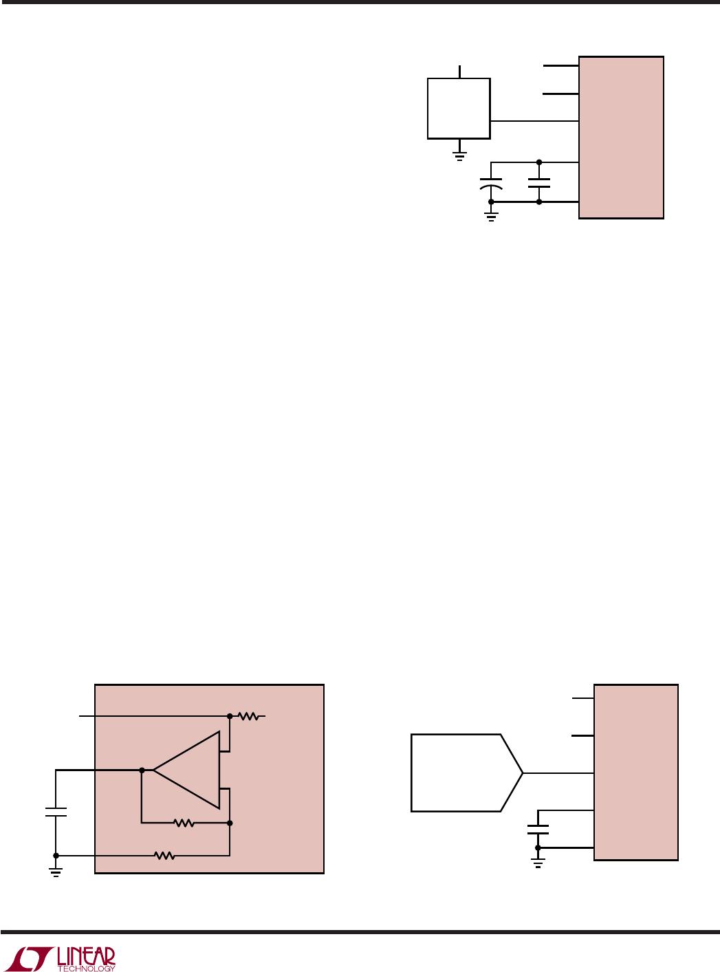
Input Filtering
The noise and the distortion of the input amplifier and
other circuitry must be considered since they will add to
the LTC1419 noise and distortion. The small-signal band-
width of the sample-and-hold circuit is 20MHz. Any noise
or distortion products that are present at the analog inputs
will be summed over this entire bandwidth. Noisy input
circuitry should be filtered prior to the analog inputs to
minimize noise. A simple 1-pole RC filter is sufficient for
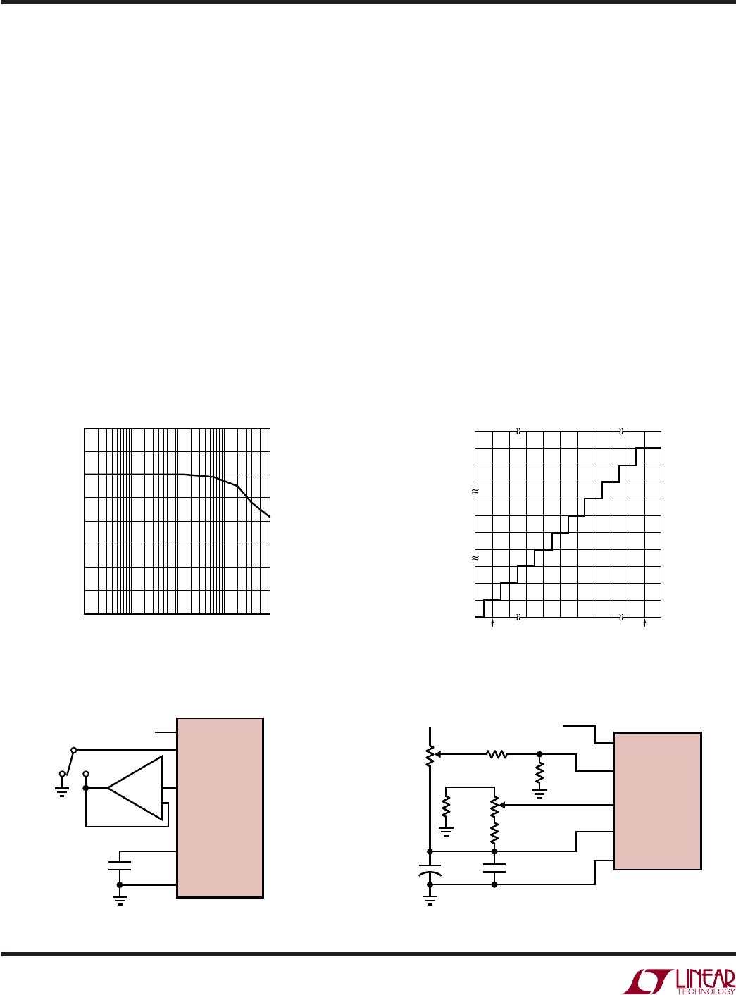
SOURCE RESISTANCE (k)
0.01
ACQUISITION TIME (µs)
1
1419 F06
0.1
0.01
0.1
110
100
10
Figure 6. t
ACQ
vs Source Resistance
Choosing an Input Amplifier
Choosing an input amplifier is easy if a few requirements
are taken into consideration. First, to limit the magnitude
of the voltage spike seen by the amplifier from charging
the sampling capacitor, choose an amplifier that has a
low output impedance (<100) at the closed-loop band-
width frequency. For example, if an amplifier is used in a
gain of +1 and has a unity-gain bandwidth of 50MHz, then
the output impedance at 50MHz should be less than
100. The second requirement is that the closed-loop
bandwidth must be greater than 20MHz to ensure
adequate small-signal settling for full throughput rate. If
slower op amps are used, more settling time can be
provided by increasing the time between conversions.
The best choice for an op amp to drive the LTC1419 will
depend on the application. Generally applications fall into
two categories: AC applications where dynamic specifi-
cations are most critical and time domain applications
where DC accuracy and settling time are most critical.
The following
list is a summary of the op amps that are
suitable for driving the LTC1419. More detailed informa-
tion is available in the Linear Technology databooks, the
LinearView
TM
CD-ROM and on our web site at www.linear-
tech. com.
Figure 7. RC Input Filter
LTC1419
+A
IN
–A
IN
V
REF
REFCOMP
AGND
1419 F07
1
2
3
4
5
10µF
1000pF
50
ANALOG INPUT
LinearView is a trademark of Linear Technology Corporation.
11
LTC1419
1419fb
many applications. For example, Figure 7 shows a 1000pF
capacitor from +A
IN
to ground and a 100 source resistor
to limit the input bandwidth to 1.6MHz. The 1000pF
capacitor also acts as a charge reservoir for the input
sample-and-hold and isolates the ADC input from sam-
pling glitch sensitive circuitry. High quality capacitors and
resistors should be used since these components can add
distortion. NPO and silver mica type dielectric capacitors
have excellent linearity. Carbon surface mount resistors can
also generate distortion from self heating and from damage
that may occur during soldering. Metal film surface mount
resistors are much less susceptible to both problems.
Input Range
The ±2.5V input range of the LTC1419 is optimized for low
noise and low distortion. Most op amps also perform well
over this same range, allowing direct coupling to the
analog inputs and eliminating the need for special transla-
tion circuitry.
Some applications may require other input ranges. The
LTC1419 differential inputs and reference circuitry can
accommodate other input ranges often with little or no
additional circuitry. The following sections describe the
reference and input circuitry and how they affect the input
range.
Internal Reference
The LTC1419 has an on-chip, temperature compensated,
curvature corrected, bandgap reference that is factory
trimmed to 2.500V. It is connected internally to a reference
amplifier and is available at V
REF
(Pin 3) see Figure 8a. A
APPLICATIONS INFORMATION
WUU
U
1
2
3
0.1µF10µF
ANALOG
INPUT
1419 F08b
LT1019A-2.5
V
OUT
V
IN
5V
+A
IN
–A
IN
V
REF
LTC1419
AGND
REFCOMP
5
4
+
Figure 8b. Using the LT1019-2.5 as an External Reference
2k resistor is in series with the output so that it can be
easily overdriven by an external reference or other
circuitry, see Figure 8b. The reference amplifier gains the
voltage at the V
REF
pin by 1.625 to create the required
internal reference voltage. This provides buffering be-
tween the V
REF
pin and the high speed capacitive DAC. The
reference amplifier compensation pin (REFCOMP, Pin 4)
must be bypassed with a capacitor to ground. The refer-
ence amplifier is stable with capacitors of 1µF or greater.
For the best noise performance, a 10µF ceramic or 10µF
tantalum in parallel with a 0.1µF ceramic is recommended.
The V
REF
pin can be driven with a DAC or other means
shown in Figure 9. This is useful in applications where the
peak input signal amplitude may vary. The input span of
the ADC can then be adjusted to match the peak input
signal, maximizing the signal-to-noise ratio. The filtering
of the internal LTC1419 reference amplifier will limit the
bandwidth and settling time of this circuit. A settling time
of 5ms should be allowed for after a reference adjustment.
Figure 8a. LTC1419 Reference Circuit
Figure 9. Driving V
REF
with a DAC
LTC1419
+A
IN
ANALOG INPUT
1.25V TO 3V
DIFFERENTIAL
–A
IN
V
REF
REFCOMP
AGND
1419 F09
1
2
3
4
5
10µF
LTC1450
1.25V TO 3V
R2
40k
R3
64k
REFERENCE
AMP
10µF
REFCOMP
AGND
V
REF
R1
2k
BANDGAP
REFERENCE
3
4
5
2.500V
4.0625V
LTC1419
1419 F08a
12
LTC1419
1419fb
APPLICATIONS INFORMATION
WUU
U
Differential Inputs
The LTC1419 has a unique differential sample-and-hold
circuit that allows rail-to-rail inputs. The ADC will always
convert the difference of +A
IN
– (–A
IN
) independent of the
common mode voltage (see Figure 11a). The common
mode rejection holds up to extremely high frequencies,
see Figure 10a. The only requirement is that both inputs
can not exceed the AV
DD
or AV
SS
power supply voltages.
Integral nonlinearity errors (INL) and differential nonlin-
earity errors (DNL) are independent of the common mode
voltage, however, the bipolar zero error (BZE) will vary.
The change in BZE is typically less than 0.1% of the
common mode voltage. Dynamic performance is also
affected by the common mode voltage. THD will degrade
as the inputs approach either power supply rail, from 86dB
with a common mode of 0V to 76dB with a common mode
of 2.5V or –2.5V.
Figure 10b. Selectable 0V to 5V or ±2.5V Input Range
Differential inputs allow greater flexibility for accepting
different input ranges. Figure 10b shows a circuit that
converts a 0V to 5V analog input signal with only an
additional buffer that is not in the signal path.
Full-Scale and Offset Adjustment
Figure 11a shows the ideal input/output characteristics
for the LTC1419. The code transitions occur midway
between successive integer LSB values (i.e., –FS +
0.5LSB, –FS + 1.5LSB, –FS + 2.5LSB,... FS – 1.5LSB,
FS –
0.5LSB). The output is two’s complement binary with
1LSB = FS – (–FS)/16384 = 5V/16384 = 305.2µV.
In applications where absolute accuracy is important,
offset and full-scale errors can be adjusted to zero. Offset
error must be adjusted before full-scale error. Figure 11b
shows the extra components required for full-scale error
adjustment. Zero offset is achieved by adjusting the offset
ANALOG
INPUT
1419 F11b
1
2
3
R4
100
R7
50k
R3
24k
5V
R6
24k
R8
50k
R5
47k
4
5
0.1µF
10µF
+A
IN
–A
IN
V
REF
REFCOMP
AGND
LTC1419
+
Figure 11b. Offset and Full-Scale Adjust Circuit
Figure 10a. CMRR vs Input Frequency
Figure 11a. LTC1419 Transfer Characteristics
1419 F11a
011...111
011...110
000...001
000...000
111...111
111...110
100...001
100...000
FS – 1LSB
(FS – 1LSB)
INPUT VOLTAGE [+A
IN
– (–A
IN
)]
OUTPUT CODE
INPUT FREQUENCY (Hz)
1
COMMON MODE REJECTION (dB)
80
70
60
50
40
30
20
10
0
10 100
1419 G09
1000 10000
LTC1419
+A
IN
ANALOG INPUT
–A
IN
V
REF
0V TO
5V
REFCOMP
AGND
1419 F10
1
2
3
±2.5V
4
5
10µF
+

LTC1419IG#PBF

Mfr. #:
Manufacturer:
Analog Devices Inc.
Description:
Analog to Digital Converters - ADC 800ksps 14-Bit Parallel ADC
Lifecycle:
New from this manufacturer.
Delivery:
DHL FedEx Ups TNT EMS
Payment:
T/T Paypal Visa MoneyGram Western Union