8308I Data Sheet
©2015 Integrated Device Technology, Inc December 10, 201510
APPLICATION INFORMATION
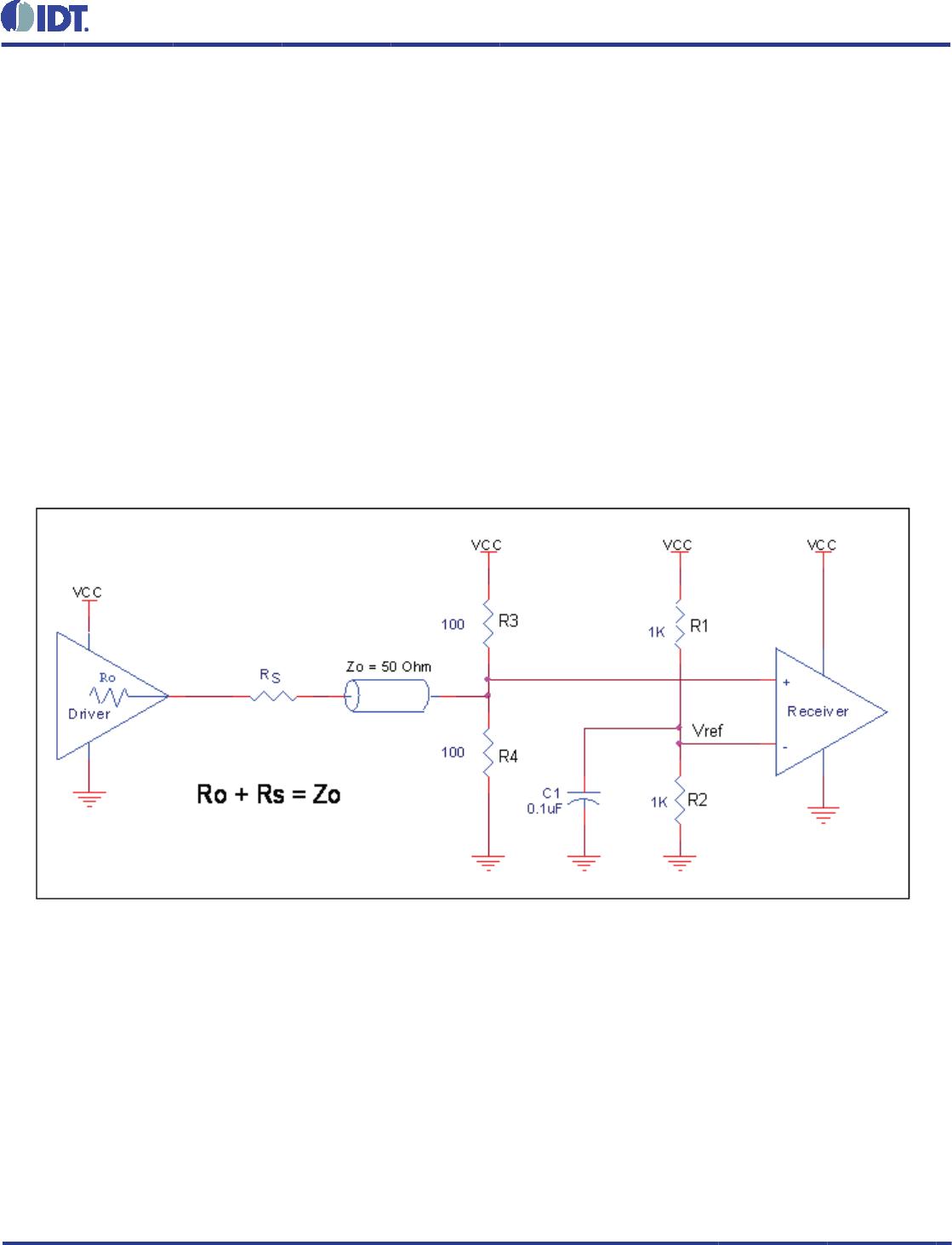
Figure 1 shows how a differential input can be wired to accept single
ended levels. The reference voltage V
REF
= V
DD
/2 is generated by
the bias resistors R1 and R2. The bypass capacitor (C1) is used to
help fi lter noise on the DC bias. This bias circuit should be located
as close to the input pin as possible. The ratio of R1 and R2 might
need to be adjusted to position the V
REF
in the center of the input
voltage swing. For example, if the input clock swing is 2.5V and V
DD
= 3.3V, R1 and R2 value should be adjusted to set V
REF
at 1.25V.
The values below are for when both the single-ended swing and V
DD
are at the same voltage. This confi guration requires that the sum of
the output impedance of the driver (Ro) and the series resistance
(Rs) equals the transmission line impedance. In addition, matched
termination at the input will attenuate the signal in half. This can be
done in one of two ways. First, R3 and R4 in parallel should equal the
FIGURE 1. RECOMMENDED SCHEMATIC FOR WIRING A DIFFERENTIAL INPUT TO ACCEPT SINGLE-ENDED LEVELS
WIRING THE DIFFERENTIAL INPUT TO ACCEPT SINGLE ENDED LEVELS
transmission line impedance. For most 50 applications, R3 and R4
can be 100Ω. The values of the resistors can be increased to reduce
the loading for slower and weaker LVCMOS driver. When using
single ended signaling, the noise rejection benefi ts of differential
signaling are reduced. Even though the differential input can handle
full rail LVCMOS signaling, it is recommended that the amplitude
be reduced. The datasheet specifi es a lower differential amplitude,
however this only applies to differential signals. For single-ended
applications, the swing can be larger, however V
IL
cannot be less
than -0.3V and V
IH
cannot be more than V
DD
+ 0.3V. Though some of
the recommended components might not be used, the pads should
be placed in the layout. They can be utilized for debugging purposes.
The datasheet specifi cations are characterized and guaranteed by
using a differential signal.
8308I Data Sheet
©2015 Integrated Device Technology, Inc December 10, 201511
3.3V
R1
50
R3
50
Zo = 50 Ohm
LVPECL
Zo = 50 Ohm
HiPerClockS
CLK
nCLK
3.3V
Input
R2
50
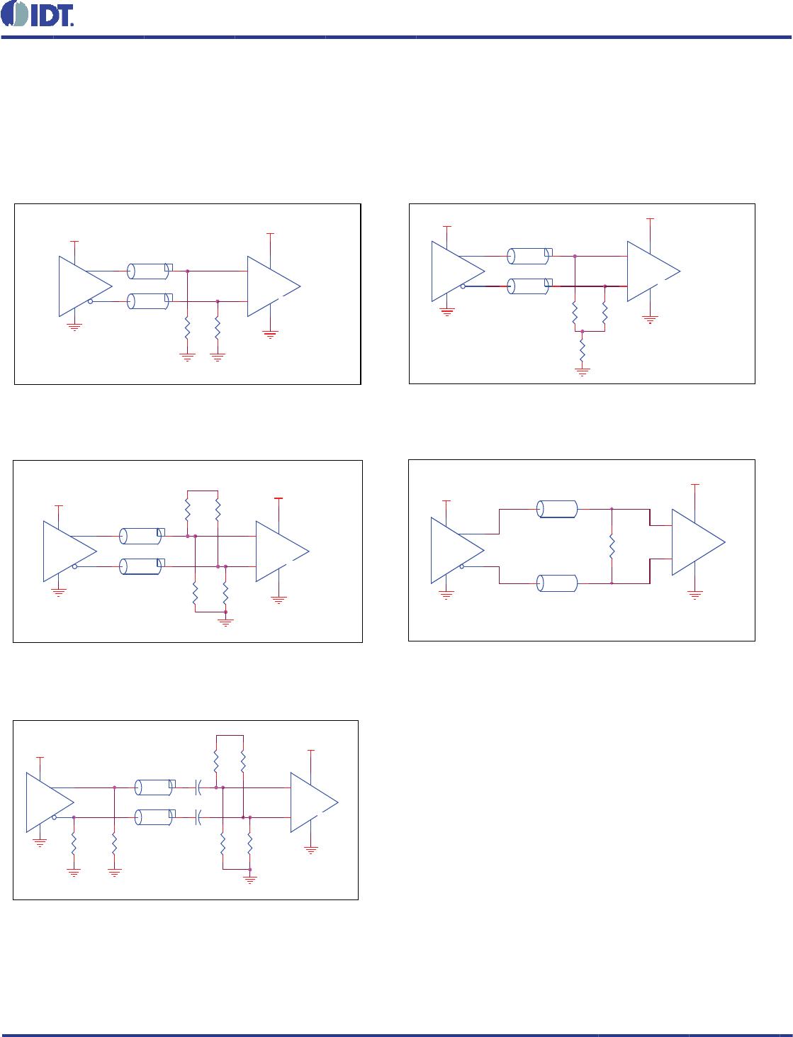
FIGURE 2C. CLK/nCLK INPUT DRIVEN BY
3.3V LVPECL DRIVER
FIGURE 2B. CLK/nCLK INPUT DRIVEN BY
3.3V LVPECL DRIVER
FIGURE 2D. CLK/nCLK INPUT DRIVEN BY
3.3V LVDS DRIVER
DIFFERENTIAL CLOCK INPUT INTERFACE
The CLK /nCLK accepts LVDS, LVPECL, LVHSTL, SSTL, HCSL
and other differential signals. Both differential signals must meet the
V
PP and VCMR input requirements. Figures 2A to 2E show interface
examples for the CLK/nCLK input driven by the most common
driver types. The input interfaces suggested here are examples
FIGURE 2A. CLK/nCLK INPUT DRIVEN BY
IDT’S LVHSTL DRIVER
only. Please consult with the vendor of the driver component to
confi rm the driver termination requirements. For example in Figure
2A, the input termination applies for IDT LVHSTL drivers. If you are
using an LVHSTL driver from another vendor, use their termination
recommendation.
FIGURE 2E. CLK/nCLK INPUT DRIVEN BY
3.3V LVPECL DRIVER WITH AC COUPLE
Zo = 50 Ohm
R1
100
3.3V
LVDS_Driv er
Zo = 50 Ohm
Receiv er
CLK
nCLK
3.3V
Zo = 50 Ohm
R3
125
HiPerClockS
CLK
nCLK
3.3V
R5
100 - 200
3.3V
R2
84
3.3V
R6
100 - 200
Input
R5,R6 locate near the driver pin.
Zo = 50 Ohm
R1
84
R4
125
C2
LVPECL
C1
Zo = 50 Ohm
Input
HiPerClockS
CLK
nCLK
3.3V
R3
125
R2
84
Zo = 50 Ohm
3.3V
R4
125
LVPECL
R1
84
3.3V
1.8V
R2
50
Input
LVHSTL Driver
ICS
HiPerClockS
R1
50
LVHSTL
3.3V
Zo = 50 Ohm
Zo = 50 Ohm
HiPerClockS
CLK
nCLK
8308I Data Sheet
©2015 Integrated Device Technology, Inc December 10, 201512
SCHEMATIC EXAMPLE
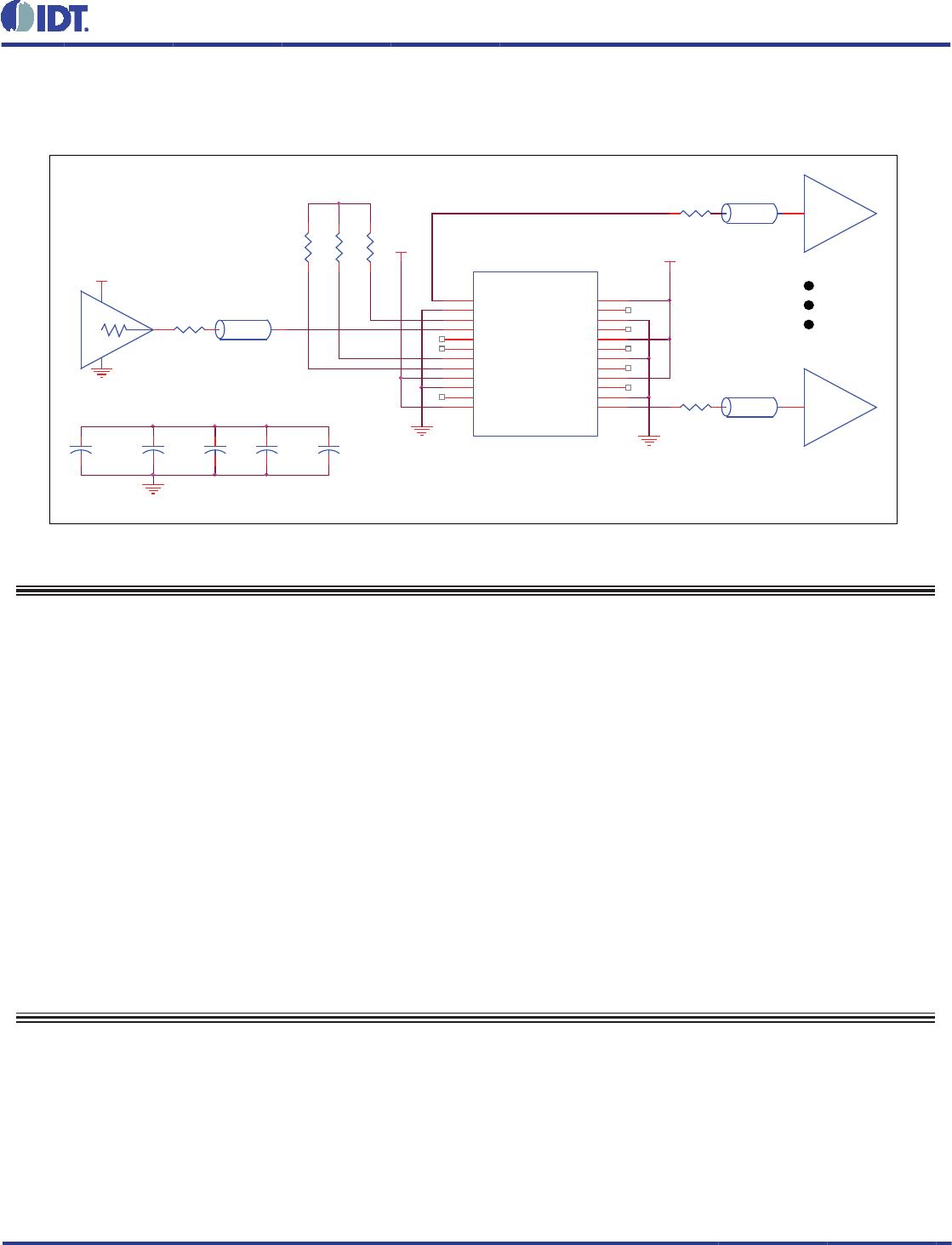
Figure 3 shows a schematic example of the 8308I. In this
example, the LVCMOS_CLK input is selected. The decoupling
FIGURE 3. 8308I LVPECL BUFFER SCHEMATIC EXAMPLE
C4
0.1u
(U1,9)
R1 43
VDD
Zo = 50 Ohm
Zo = 50 Ohm
(U1,16)
R10
1K
R11 43
C2
0.1u
C3
0.1u
VDD
(U1,20)
U1
ICS8308I
1
2
3
4
5
6
7
8
9
10
11
12 13
14
15
16
17
18
19
20
21
22
23
24
Q0
GND
CLK_SEL
LVCMOS_CLK
CLK
nCLK
CLK_EN
OE
VDD
GND
Q1
VDDO Q7
GND
Q6
VDDO
Q5
GND
Q4
VDDO
Q3
GND
Q2
VDDO
VDD=3.3V
R9
1K
(U1,12) R8 43
Ro ~ 7 Ohm
3.3V_LVCMOS
3.3V LVCMOS/LVTTL
C5
0.1u
R12
1K
VDD
(U1,24)
Zo = 50 Ohm
VDD
VDD
3.3V LVCMOS/LVTTL
C1
0.1u
capacitors should be physically located near the power pin.
INPUTS:
LVCMOS_CLK I
NPUT
For applications not requiring the use of an LVCMOS_CLK, it can
be left fl oating. Though not required, but for additional protection,
a 1kΩ resistor can be tied from the LVCMOS_CLK input to ground.
CLK/nCLK I
NPUTS
For applications not requiring the use of the differential input, both
CLK and nCLK can be left fl oating. Though not required, but for
additional protection, a 1kΩ resistor can be tied from CLK to ground.
LVCMOS C
ONTROL PINS
All control pins have internal pullups or pulldowns; additional
resistance is not required but can be added for additional protection.
A 1kΩ resistor can be used.
RECOMMENDATIONS FOR UNUSED INPUT AND OUTPUT PINS
OUTPUTS:
LVCMOS OUTPUTS
All unused LVCMOS outputs can be left fl oating. There should be
no trace attached.
Power On Sequence
There is no power on sequence requirement for the V
DD
and V
DDO.
If the V
DDO
is turned on before the V
DD,
there will be unknown state
at the outputs during initial condition when the V
DDO
is on and V
DD
is off.

8308AGILFT

Mfr. #:
Manufacturer:
IDT
Description:
Clock Buffer 1:8 Differential/LVC MOS to LVCMOS Fanout
Lifecycle:
New from this manufacturer.
Delivery:
DHL FedEx Ups TNT EMS
Payment:
T/T Paypal Visa MoneyGram Western Union

Products related to this Datasheet