8308I Data Sheet
©2015 Integrated Device Technology, Inc December 10, 20154
TABLE 4D. DC CHARACTERISTICS, V
DD
= V
DDO
= 3.3V±5%, TA = -40° TO 85°
Symbol Parameter Test Conditions Minimum Typical Maximum Units
V
IH
Input High Voltage LVCMOS 2 V
DD
+ 0.3 V
V
IL
Input Low Voltage
LVCMOS_CLK -0.3 1.3 V
CLK_EN, OE 0.8 V
I
IN
Input Current V
IN
= V
DD
or V
IN
= GND 300 µA
V
OH
Output High Voltage; NOTE 1 I
OH
= -24mA 2.4 V
V
OL
Output Low Voltage; NOTE 1
I
OL
= 24mA 0.55 V
I
OL
= 12mA 0.30 V
V
PP
Peak-to-Peak Input Voltage CLK, nCLK 0.15 1.3 V
V
CMR
Input Common Mode Voltage;
NOTE 2, 3
CLK, nCLK GND + 0.5 V
DD
- 0.85 V
NOTE 1: Outputs capable of driving 50Ω transmission lines terminated with 50Ω to V
DDO
/2.
See Parameter Measurement section, “3.3V Output Load AC Test Circuit”.
NOTE 2: For single ended applications, the maximum input voltage for CLK, nCLK is
V
DD
+ 0.3V.
NOTE 3: Common mode voltage is defi ned as
V
IH
.
TABLE 4E. DC CHARACTERISTICS, V
DD
= 3.3V±5%, V
DDO
= 2.5V±5%, TA = -40° TO 85°
Symbol Parameter Test Conditions Minimum Typical Maximum Units
V
IH
Input High Voltage LVCMOS 2 V
DD
+ 0.3 V
V
IL
Input Low Voltage
LVCMOS_CLK -0.3 1.3 V
CLK_EN, OE 0.8 V
I
IN
Input Current V
IN
= V
DD
or V
IN
= GND 300 µA
V
OH
Output High Voltage; NOTE 1 I
OH
= -15mA 1.8 V
V
OL
Output Low Voltage; NOTE 1 I
OL
= 15mA 0.6 V
V
PP
Peak-to-Peak Input Voltage CLK, nCLK 0.15 1.3 V
V
CMR
Input Common Mode Voltage;
NOTE 2, 3
CLK, nCLK GND + 0.5 V
DD
- 0.85 V
NOTE 1: Outputs capable of driving 50Ω transmission lines terminated with 50Ω to V
DDO
/2.
See Parameter Measurement section, “3.3V Output Load AC Test Circuit”.
NOTE 2: For single ended applications, the maximum input voltage for CLK, nCLK is
V
DD
+ 0.3V.
NOTE 3: Common mode voltage is defi ned as
V
IH
.
8308I Data Sheet
©2015 Integrated Device Technology, Inc December 10, 20155
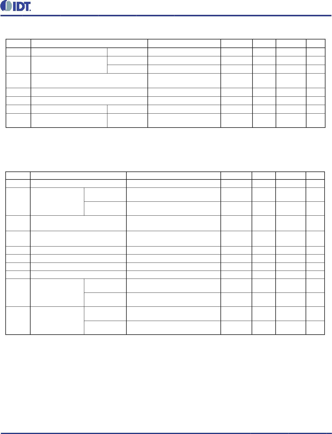
TABLE 4F. DC CHARACTERISTICS, V
DD
, V
DDO
= 2.5V±5%, TA = -40° TO 85°
TABLE 5A. AC CHARACTERISTICS, V
DD
= V
DDO
= 3.3V±5%, TA = -40° TO 85°
Symbol Parameter Test Conditions Minimum Typical Maximum Units
V
IH
Input High Voltage LVCMOS 1.7 V
DD
+ 0.3 V
V
IL
Input Low Voltage
LVCMOS_CLK -0.3 0.7 V
CLK_EN, OE 0.7 V
I
IN
Input Current V
IN
= V
DD
or V
IN
= GND 300 µA
V
OH
Output High Voltage; NOTE 1 I
OH
= -15mA 1.8 V
V
OL
Output Low Voltage; NOTE 1 I
OL
= 15mA 0.6 V
V
PP
Peak-to-Peak Input Voltage CLK, nCLK 0.15 1.3 V
V
CMR
Input Common Mode Voltage;
NOTE 2, 3
CLK, nCLK GND + 0.5 V
DD
- 0.85 V
NOTE 1: Outputs capable of driving 50Ω transmission lines terminated with 50Ω to V
DDO
/2.
See Parameter Measurement section, “3.3V Output Load AC Test Circuit”.
NOTE 2: For single ended applications, the maximum input voltage for CLK, nCLK is
V
DD
+ 0.3V.
NOTE 3: Common mode voltage is defi ned as
V
IH
.
Symbol Parameter Test Conditions Minimum Typical Maximum Units
f
OUT
Output Frequency 350 MHz
t
PD
Propagation Delay;
CLK, nCLK;
NOTE 1
ƒ 350MHz 2 4 ns
LVCMOS_CLK;
NOTE 2
ƒ 350MHz 2 4 ns
tsk(o) Output Skew; NOTE 3, 7 Measured on rising edge @V
DDO
/2 100 ps
tsk(pp) Part-to-Part Skew; NOTE 4, 7 Measured on rising edge @V
DDO
/2 1 ns
t
R
/ t
F
Output Rise/Fall Time 0.8V to 2V 0.2 1 ns
odc Output Duty Cycle
ƒ 150MHz, Ref = CLK, nCLK
45 55 %
t
PZL
, t
PZH
Output Enable Time; NOTE 5 5ns
t
PLZ
, t
PHZ
Output Disable Time; NOTE 5 5ns
t
S
Clock Enable
Setup Time;
NOTE 6
CLK_EN to CLK,
nCLK
1ns
CLK_EN to LVC-
MOS_CLK
0ns
t
H
Clock Enable
Hold Time;
NOTE 6
CLK, nCLK to
CLK_EN
0ns
LVCMOS_CLK
to CLK_EN
1ns
NOTE: Electrical parameters are guaranteed over the specifi ed ambient operating temperature range, which is established when the
device is mounted in a test socket with maintained transverse airfl ow greater than 500 lfpm. The device will meet specifi cations after
thermal equilibrium has been reached under these conditions.
NOTE 1: Measured from the differential input crossing point to V
DDO
/2 of the output.
NOTE 2: Measured from V
DD
/2 of the input to V
DDO
/2 of the output.
NOTE 3: Defi ned as skew between outputs at the same supply voltage and with equal load conditions.
Measured at V
DDO
/2.
NOTE 4: Defi ned as skew between outputs on different devices operating at the same supply voltages and with
equal load conditions. Using the same type of inputs on each device, the outputs are measured at V
DDO
/2.
NOTE 5: These parameters are guaranteed by characterization. Not tested in production.
NOTE 6: Setup and Hold times are relative to the rising edge of the input clock.
NOTE 7: This parameter is defi ned in accordance with JEDEC Standard 65.
8308I Data Sheet
©2015 Integrated Device Technology, Inc December 10, 20156
TABLE 5B. AC CHARACTERISTICS, V
DD
= 3.3V±5%, V
DDO
= 2.5V±5%, TA = -40° TO 85°
Symbol Parameter Test Conditions Minimum Typical Maximum Units
f
OUT
Output Frequency 350 MHz
t
PD
Propagation Delay;
CLK, nCLK;
NOTE 1
ƒ 350MHz
24ns
LVCMOS_CLK;
NOTE 2
ƒ 350MHz
24ns
tsk(o) Output Skew; NOTE 3, 7 Measured on rising edge @V
DDO
/2 100 ps
tsk(pp) Part-to-Part Skew; NOTE 4, 7 Measured on rising edge @V
DDO
/2 1 ns
t
R
/ t
F
Output Rise/Fall Time 0.6V to 1.8V 0.2 1.0 ns
odc Output Duty Cycle
ƒ 150MHz, Ref = CLK, nCLK
45 55 %
t
PZL
, t
PZH
Output Enable Time; NOTE 5 5ns
t
PLZ
, t
PHZ
Output Disable Time; NOTE 5 5ns
t
S
Clock Enable
Setup Time;
NOTE 6
CLK_EN to CLK,
nCLK
1ns
CLK_EN to LVC-
MOS_CLK
0ns
t
H
Clock Enable
Hold Time;
NOTE 6
CLK, nCLK to
CLK_EN
0ns
LVCMOS_CLK
to CLK_EN
1ns
NOTE: Electrical parameters are guaranteed over the specifi ed ambient operating temperature range, which is established when the
device is mounted in a test socket with maintained transverse airfl ow greater than 500 lfpm. The device will meet specifi cations after
thermal equilibrium has been reached under these conditions.
NOTE 1: Measured from the differential input crossing point to V
DDO
/2 of the output.
NOTE 2: Measured from V
DD
/2 of the input to V
DDO
/2 of the output.
NOTE 3: Defi ned as skew between outputs at the same supply voltage and with equal load conditions.
Measured at V
DDO
/2.
NOTE 4: Defi ned as skew between outputs on different devices operating at the same supply voltages and with
equal load conditions. Using the same type of inputs on each device, the outputs are measured at V
DDO
/2.
NOTE 5: These parameters are guaranteed by characterization. Not tested in production.
NOTE 6: Setup and Hold times are relative to the rising edge of the input clock.
NOTE 7: This parameter is defi ned in accordance with JEDEC Standard 65.

8308AGILFT

Mfr. #:
Manufacturer:
IDT
Description:
Clock Buffer 1:8 Differential/LVC MOS to LVCMOS Fanout
Lifecycle:
New from this manufacturer.
Delivery:
DHL FedEx Ups TNT EMS
Payment:
T/T Paypal Visa MoneyGram Western Union

Products related to this Datasheet