1
100V, 2A Peak, High Frequency Half-Bridge Drivers with
Adjustable Dead Time Control and PWM Input
HIP2120, HIP2121
The HIP2120 and HIP2121 are 100V, high frequency, half-bridge
MOSFET driver ICs. They are based on the popular ISL2100A and
ISL2101A half-bridge drivers.
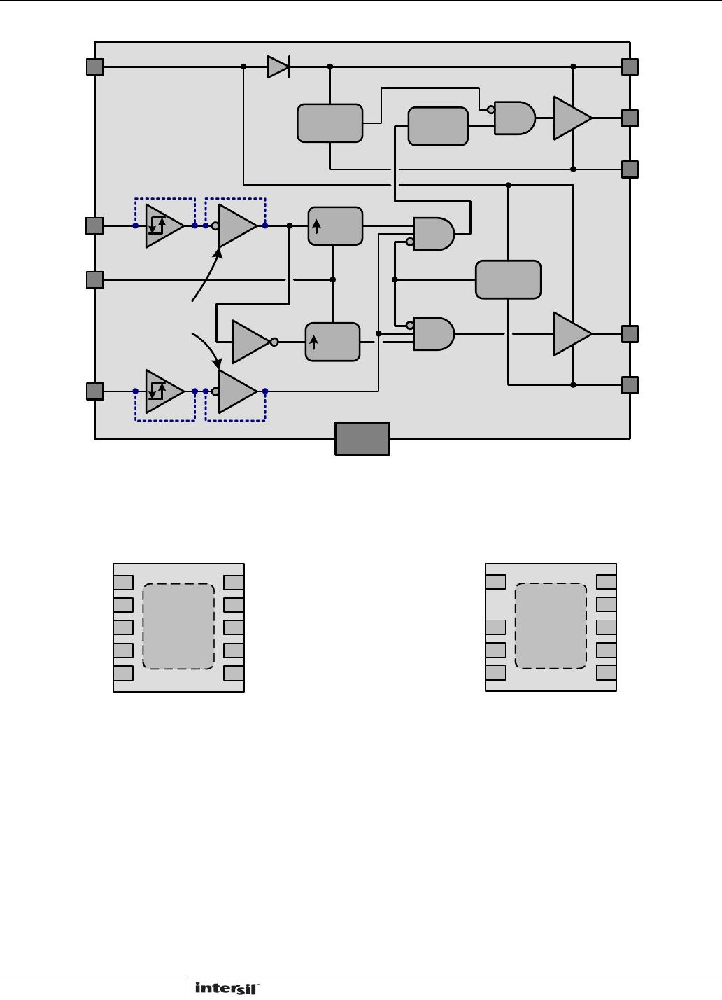
These drivers have a programmable dead-time to insure
break-before-make operation between the high-side and low-side
drivers. The dead-time is adjustable up to 250ns.
A single PWM logic input controls both bridge outputs (HO, LO). An
enable pin (EN), when low, drives both outputs to a low state. All
logic inputs are V
DD
tolerant and the HIP2120 has CMOS inputs
with hysteresis for superior operation in noisy environments.
The HIP2120 has hysteretic inputs with thresholds that are
proportional to V
DD
. The HIP2121 has 3.3V logic/TTL compatible
inputs.
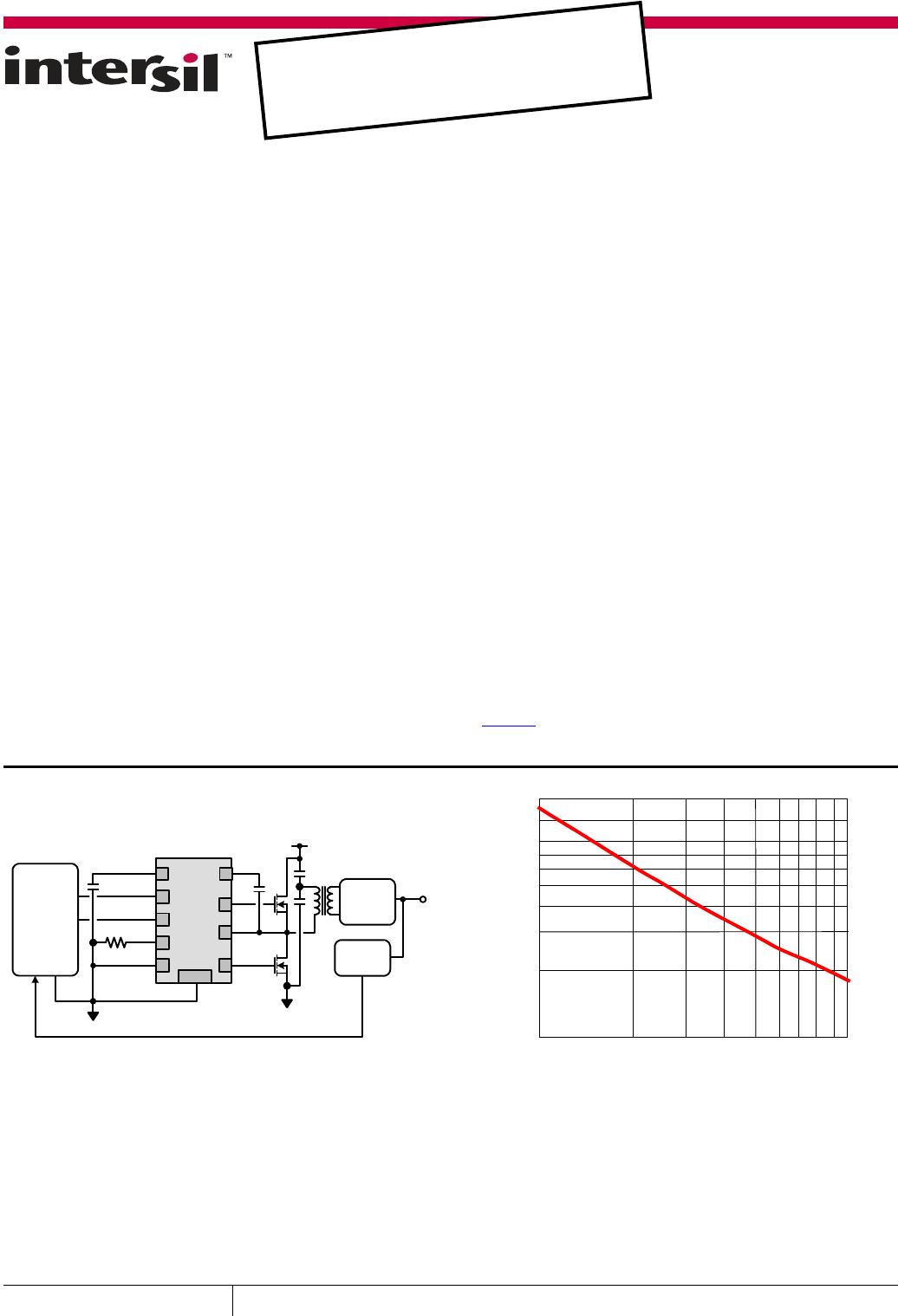
Two package options are provided. The 10 Ld 4x4 DFN package has
standard pinouts. The 9 Ld 4x4 DFN package omits pin 2 to comply
with 100V conductor spacing per IPC-2221.
Features
9 Ld TDFN “B” Package Compliant with 100V Conductor
Spacing Guidelines per IPC-2221
Break-Before-Make Dead-Time Prevents Shoot-through and is
adjustable up to 220ns
Bootstrap Supply Max Voltage to 114VDC
Wide Supply Voltage Range (8V to 14V)
Supply Undervoltage Protection
CMOS Compatible Input Thresholds with Hysteresis (HIP2120)
•1.6/1 Typical Output Pull-up/Pull-down Resistance
•On-Chip 1 Bootstrap Diode
Applications
Telecom Half-Bridge DC/DC Converters
•UPS and Inverters
•Motor Drives
Class-D Amplifiers
Forward Converter with Active Clamp
Related Literature
FN7670 “HIP2122, HIP2123 100V, 2A Peak, High Frequency
Half-Bridge Driver with Delay Timers”
FIGURE 1. TYPICAL APPLICATION FIGURE 2. DEAD-TIME vs TIMING RESISTOR
VDD HB
HO
HS
LOVSS
PWM
EN
100V max
RDT
FEEDBACK
WITH
ISOLATION
PWM
CONTROLLER
SECONDARY
CIRCUITS
HIP2120/21
EPAD
HALF BRIDGE
R
DT
(k)
8162432485640 64 80
DEAD-TIME (ns)
200
160
140
120
100
80
60
40
20
CAUTION: These devices are sensitive to electrostatic discharge; follow proper IC Handling Procedures.
1-888-INTERSIL or 1-888-468-3774
|Copyright Intersil Americas Inc. 2011. All Rights Reserved
Intersil (and design) is a trademark owned by Intersil Corporation or one of its subsidiaries.
All other trademarks mentioned are the property of their respective owners.
December 23, 2011
FN7668.0
N
O
T
R
E
C
O
M
M
E
N
D
E
D
F
O
R
N
E
W
D
E
S
I
G
N
S
N
O
R
E
C
O
M
M
E
N
D
E
D
R
E
P
L
A
C
E
M
E
N
T
c
o
n
t
a
c
t
o
u
r
T
e
c
h
n
i
c
a
l
S
u
p
p
o
r
t
C
e
n
t
e
r
a
t
1
-8
8
8
-
I
N
T
E
R
S
I
L
o
r
w
w
w
.
i
n
te
r
s
i
l
.
c
o
m
/
t
s
c
HIP2120, HIP2121
2
FN7668.0
December 23, 2011
Block Diagram
Pin Configurations
HIP2120, HIP2121
(10 LD 4X4 TDFN)
TOP VIEW
HIP2120, HIP2121
(9 LD 4X4 TDFN)
TOP VIEW
LEVEL
SHIFT
UNDER
VOLTAGE
UNDER
VOLTAGE
EPAD
DELAY
HIP2120,
HIP2121
HIP2121
HIP2121
HIP2120/21
HIP2120/21
Optional
inversion
for future
part
numbers
VDD
PWM
RDT
EN
HB
HO
HS
LO
VSS
DELAY
EPAD IS
ELECTRICALLY
ISOLATED
EPAD
1
2
3
4
5
10
9
8
7
6
VDD
HB
HO
HS
NC
LO
VSS
PWM
EN
RDT
EPAD
1
3
4
5
10
9
8
7
6
VDD
HB
HO
HS
LO
VSS
PWM
EN
RDT
HIP2120, HIP2121
3
FN7668.0
December 23, 2011
Pin Descriptions
10 LD 9 LD SYMBOL DESCRIPTION
1 1 VDD Positive supply voltage for lower gate driver. Decouple this pin with a ceramic capacitor to
VSS.
2 3 HB High-side bootstrap supply voltage referenced to HS. Connect the positive side of the
bootstrap capacitor to this pin. Bootstrap diode is on-chip.
3 4 HO High-side output. Connect to gate of high-side power MOSFET.
4 5 HS High-side source connection. Connect to source of high-side power MOSFET. Connect
negative side of bootstrap capacitor to this pin.
8 8 PWM PWM input. For PWM = 1, HO = 1 and LO = 0. For PWM = 0, HO = 0 and LO = 1.
7 7 EN Output enable, when low, HO = LO = 0
9 9 VSS Negative voltage supply, which will generally be ground.
10 10 LO Low-side output. Connect to gate of low-side power MOSFET.
5 - NC No Connect. This pin is isolated from all other pins.
6 6 RDT A resistor connected between this pin and VSS adds additional delay time to the falling and
rising edges of the PWM input.
- - EPAD Exposed pad. Connect to ground or float. The EPAD is electrically isolated from all other
pins.
Ordering Information
PART NUMBER
(Notes 1, 2, 4)
PART
MARKING INPUT
TEMP. RANGE
(°C)
PACKAGE
(Pb-Free)
PKG.
DWG. #
HIP2120FRTAZ HIP 2120AZ CMOS -40 +125 10 Ld 4x4 TDFN L10.4x4
HIP2121FRTAZ HIP 2121AZ 3.3V/TTL -40 +125 10 Ld 4x4 TDFN L10.4x4
HIP2120FRTBZ (Note 3) HIP 2120BZ CMOS -40 +125 9 Ld 4x4 TDFN L9.4x4
HIP2121FRTBZ (Note 3) HIP 2121BZ 3.3V/TTL -40 +125 9 Ld 4x4 TDFN L9.4x4
NOTES:
1. Please refer to TB347
for details on reel specifications.
2. These Intersil Pb-free plastic packaged products employ special Pb-free material sets, molding compounds/die attach materials, and 100% matte
tin plate plus anneal (e3 termination finish, which is RoHS compliant and compatible with both SnPb and Pb-free soldering operations). Intersil
Pb-free products are MSL classified at Pb-free peak reflow temperatures that meet or exceed the Pb-free requirements of IPC/JEDEC J STD-020.
3. “B” package option has alternate pin assignments for compliance with 100V Conductor Spacing Guidelines per IPC-2221. Note that Pin 2 is omitted
for additional spacing.
4. For Moisture Sensitivity Level (MSL), please see device information page for HIP2120, HIP2121
. For more information on MSL please see tech brief
TB363
.

HIP2120FRTAZ

Mfr. #:
Manufacturer:
Renesas / Intersil
Description:
Gate Drivers 100V 2A PEAK HALF BRDG DRV W/DELAY TMR
Lifecycle:
New from this manufacturer.
Delivery:
DHL FedEx Ups TNT EMS
Payment:
T/T Paypal Visa MoneyGram Western Union