HIP2120, HIP2121
5
FN7668.0
December 23, 2011
Absolute Maximum Ratings Thermal Information
Supply Voltage, V
DD
, V
HB
- V
HS
(Notes 5, 6) . . . . . . . . . . . . . . . -0.3V to 18V
PWM and EN Input Voltage (Note 6) . . . . . . . . . . . . . . .-0.3V to VDD + 0.3V
Voltage on LO (Note 6) . . . . . . . . . . . . . . . . . . . . . . . . . . .-0.3V to VDD + 0.3V
Voltage on HO (Note 6) . . . . . . . . . . . . . . . . . . . . . VHS - 0.3V to VHB + 0.3V
Voltage on HS (Continuous) (Note 6) . . . . . . . . . . . . . . . . . . . . . -1V to 110V
Voltage on HB (Note 6). . . . . . . . . . . . . . . . . . . . . . . . . . . . . . . . . . . . . . . 118V
Average Current in V
DD
to HB Diode . . . . . . . . . . . . . . . . . . . . . . . . . 100mA
Maximum Recommended Operating
Conditions
Supply Voltage, V
DD
. . . . . . . . . . . . . . . . . . . . . . . . . . . . . . . . . . . . . 8V to 14V
Voltage on HS . . . . . . . . . . . . . . . . . . . . . . . . . . . . . . . . . . . . . . . . -1V to 100V
Voltage on HS . . . . . . . . . . . . . . . . . . . . . .(Repetitive Transient) -5V to 105V
Voltage on HB . . . . . . . . . . . . . . . . . . . . . . . . . . . . . . . V
HS
+ 8V to V
HS
+ 14V and
. . . . . . . . . . . . . . . . . . . . . . . . . . . . . . . . . . . . . . . . . . . . . . . V
DD
- 1V to V
DD
+ 100V
HS Slew Rate. . . . . . . . . . . . . . . . . . . . . . . . . . . . . . . . . . . . . . . . . . . . <50V/ns
Thermal Resistance (Typical)
JA
(°C/W)
JC
(°C/W)
10 Ld TDFN (Notes 7, 8) . . . . . . . . . . . . . . . 42 4
9 Ld TDFN (Notes 7, 8) . . . . . . . . . . . . . . . . 42 4
Max Power Dissipation at +25°C in Free Air
10 Ld TDFN (Notes 7, 8) . . . . . . . . . . . . . . . . . . . . . . . . . . . . . . . . . . . . . 3.0W
9 Ld TDFN (Notes 7, 8). . . . . . . . . . . . . . . . . . . . . . . . . . . . . . . . . . . . . . . 3.1W
Storage Temperature Range. . . . . . . . . . . . . . . . . . . . . . . .-65°C to +150°C
Junction Temperature Range . . . . . . . . . . . . . . . . . . . . . . .-55°C to +150°C
Pb-free reflow profile . . . . . . . . . . . . . . . . . . . . . . . . . . . . . . . . see link below
http://www.intersil.com/pbfree/Pb-FreeReflow.asp
ESD Ratings
Human Body Model Class 2 (Tested per JESD22-A114E). . . . . . . . . . 3000V
Machine Model Class B (Tested per JESD22-A115-A). . . . . . . . . . . . . . 300V
Charged Device Model Class IV. . . . . . . . . . . . . . . . . . . . . . . . . . . . . . . . 2000V
CAUTION: Do not operate at or near the maximum ratings listed for extended periods of time. Exposure to such conditions may adversely impact product
reliability and result in failures not covered by warranty.
NOTES:
5. The HIP2120 and HIP2121 are capable of derated operation at supply voltages exceeding 14V. Figure 20 shows the high-side voltage derating curve
for this mode of operation.
6. All voltages referenced to V
SS
unless otherwise specified.
7.
JA
is measured in free air with the component mounted on a high effective thermal conductivity test board with “direct attach” features. See Tech
Brief TB379
.
8. For
JC
, the “case temp” location is the center of the exposed metal pad on the package underside.
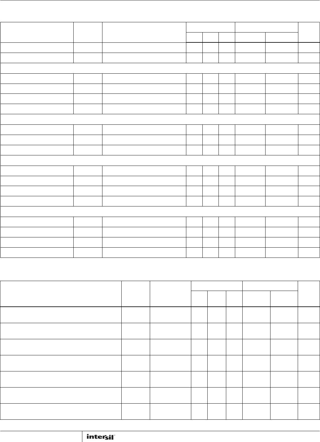
Electrical Specifications V
DD
= V
HB
= 12V, V
SS
= V
HS
= 0V, R
DT
= 0
K
, PWM = 0V, No Load on LO or HO, Unless Otherwise Specified.
Boldface limits apply over the operating temperature range, -40°C to +125°C.
PARAMETERS SYMBOL TEST CONDITIONS
T
A
= +25°C T
A
= -40°C to +125°C
UNITSMIN TYP MAX MIN (Note 9) MAX (Note 9)
SUPPLY CURRENTS
V
DD
Quiescent Current
I
DD80
R
DT
= 80k - 470 850 - 900 µA
I
DD8k
R
DT
= 8k - 1.0 2.1 - 2.2 mA
V
DD
Operating Current
I
DDO80k
f = 500kHz, R
DT
= 80k - 2.5 3 - 3 mA
I
DDO8k
f = 500kHz, R
DT
= 8k - 3.4 4 - 4 mA
Total HB Quiescent Current I
HB
LI = HI = 0V - 65 115 - 150 µA
Total HB Operating Current I
HBO
f = 500kHz - 2.0 2.5 - 3 mA
HB to V
SS
Current, Quiescent I
HBS
LI = HI = 0V; V
HB
= V
HS
= 114V - 0.05 1.5 - 10 µA
HB to V
SS
Current, Operating I
HBSO
f = 500kHz; V
HB
= V
HS
= 114V - 1.2 1.5 - 1.6 mA
INPUT PINS
Low Level Input Voltage
Threshold
V
IL
HIP2120 (CMOS) 3.7 4.4 - 2.7 -
V
Low Level Input Voltage
Threshold
V
IL
HIP2121 (3.3V/TTL) 1.4 1.8 - 1.2 -
V
High Level Input Voltage
Threshold
V
IH
HIP2120 (CMOS) - 6.54 7.93 5.3 8.2
V
High Level Input Voltage
Threshold
V
IH
HIP2121 ((3.3V/TTL) - 1.8 2.2 -2.4V