HIP2120, HIP2121
13
FN7668.0
December 23, 2011
Power Dissipation
The dissipation of the HIP2120/21 is dominated by the gate
charge required by the driven bridge FETs and the switching
frequency. The internal bias and boot diode also contribute to the
total dissipation but these losses are usually insignificant
compared to the gate charge losses.
The calculation of the power dissipation of the HIP2120/21 is
very simple.
GATE POWER (FOR THE HO AND LO OUTPUTS)
P
gate
= 4 x Q
gate
x Freq x VDD
where
Q
gate
is the charge of the driven bridge FET at VDD, and
Freq is the switching frequency.
BOOT DIODE DISSIPATION
I
diode_avg
= Q
gate
x Freq
P
diode
= I
diode_avg
x 0.6V
where 0.6V is the diode conduction voltage
BIAS CURRENT
P
bias
= I
bias
x VDD
where I
bias
is the internal bias current of the HIP2120/21 at the
switching frequency
TOTAL POWER DISSIPATION
P
total
= P
gate
+ P
diode
+ P
bias
OPERATING TEMPERATURES
T
j
= P
total
x
JA
+ T
amb
where T
j
is the junction temperature at the operating air
temperature, T
amb
, in the vicinity of the part.
T
j
= P
total
x
JC
+ T
PCB
where T
j
is the junction temperature with the operating
temperature of the PCB, T
PCB
, measured where the EPAD is
soldered.
PC Board Layout
The AC performance of the HIP2120/21 depends significantly on
the design of the PC board. The following layout design
guidelines are recommended to achieve optimum performance
from the HIP2120/21:
Understand well how power currents flow. The high amplitude
di/dt currents of the bridge FETs will induce significant voltage
transients on the associated traces.
Keep power loops as short as possible by paralleling the
source and return traces.
Use planes where practical; they’re usually more effective than
parallel traces.
Planes can also be non-grounded nodes.
Avoid paralleling high di/dt traces with low level signal lines.
High di/dt will induce currents in the low level signal lines.
When practical, minimize impedances in low level signal
circuits; the noise, magnetically induced on a 10k resistor, is
10x larger than the noise on a 1k resistor.
Be aware of magnetic fields emanating from transformers and
inductors. Core gaps in these structures are especially bad for
emitting flux.
If you must have traces close to magnetic devices, align the
traces so that they are parallel to the flux lines.
The use of low inductance components such as chip resistors
and chip capacitors is recommended.
Use decoupling capacitors to reduce the influence of parasitic
inductors. To be effective, these capacitors must also have the
shortest possible lead lengths. If vias are used, connect several
paralleled vias to reduce the inductance of the vias.
It may be necessary to add resistance to dampen resonating
parasitic circuits. The most likely circuit will be the HO and LO
outputs. In PCB designs with long leads on the LI and HI inputs,
it may also be necessary to add series resistors with the LI and
HI inputs.
Keep high dv/dt nodes away from low level circuits. Guard
banding can be used to shunt away dv/dt injected currents
from sensitive circuits. This is especially true for the PWM
control circuits.
Avoid having a signal ground plane under a high dv/dt circuit.
This will inject high di/dt currents into the signal ground paths.
Do power dissipation and voltage drop calculations of the
power traces. Most PCB/CAD programs have built in tools for
calculation of trace resistance.
Large power components (Power FETs, Electrolytic capacitors,
power resistors, etc.) will have internal parasitic inductance,
which cannot be eliminated. This must be accounted for in the
PCB layout and circuit design.
If you simulate your circuits, consider including parasitic
components.
HIP2120, HIP2121
14
Intersil products are manufactured, assembled and tested utilizing ISO9001 quality systems as noted
in the quality certifications found at www.intersil.com/design/quality
Intersil products are sold by description only. Intersil Corporation reserves the right to make changes in circuit design, software and/or specifications at any time
without notice. Accordingly, the reader is cautioned to verify that data sheets are current before placing orders. Information furnished by Intersil is believed to be
accurate and reliable. However, no responsibility is assumed by Intersil or its subsidiaries for its use; nor for any infringements of patents or other rights of third
parties which may result from its use. No license is granted by implication or otherwise under any patent or patent rights of Intersil or its subsidiaries.
For information regarding Intersil Corporation and its products, see www.intersil.com
FN7668.0
December 23, 2011
For additional products, see www.intersil.com/product_tree
EPAD Design Considerations
The thermal pad of the HIP2120/21 is electrically isolated. It’s
primary function is to provide heat sinking for the IC. It is
recommended to tie the EPAD to V
SS
(GND).
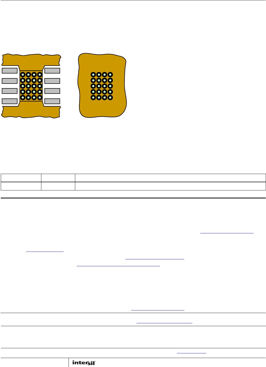
Figure 24 is an example of how to use vias to remove heat from
the IC substrate.
Depending on the amount of power dissipated by the HIP2120/21,
it may be necessary, to connect the EPAD to one or more ground
plane layers. A via array, within the area of the EPAD, will conduct
heat from the EPAD to the gnd plane on the bottom layer. If inner
PCB layers are available, it is also be desireable to connect these
additional layers with the plated-through vias.
The number of vias and the size of the GND planes required for
adequate heatsinking is determined by the power dissipated by
the HIP2120/21, the air flow, and the maximum temperature of
the air around the IC.
It is important that the vias have a low thermal resistance for
efficient heat transfer. Do not use “thermal relief” patterns to
connect the vias.
Products
Intersil Corporation is a leader in the design and manufacture of high-performance analog semiconductors. The Company's products
address some of the industry's fastest growing markets, such as, flat panel displays, cell phones, handheld products, and notebooks.
Intersil's product families address power management and analog signal processing functions. Go to www.intersil.com/products
for a
complete list of Intersil product families.
For a complete listing of Applications, Related Documentation and Related Parts, please see the respective device information page on
intersil.com: HIP2120, HIP2121
To report errors or suggestions for this datasheet, please go to: www.intersil.com/askourstaff
FITs are available from our website at: http://rel.intersil.com/reports/search.php
FIGURE 24. PCB VIA PATTERN
EPAD
GND
PLANE
COMPONENT
LAYER
EPAD
GND
PLANE
BOTTOM
LAYER
FIGURE 24. TYPICAL PCB PATTERN FOR THERMAL VIAS
Revision History
The revision history provided is for informational purposes only and is believed to be accurate, but not warranted. Please go to web to make sure you
have the latest revision.
DATE REVISION CHANGE
December 23, 2011 FN7668.0 Initial Release
HIP2120, HIP2121
15
FN7668.0
December 23, 2011
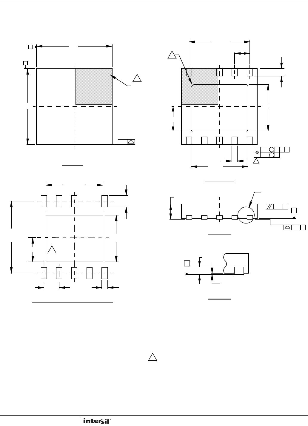
Package Outline Drawing
L9.4x4
9 LEAD THIN DUAL FLAT NO-LEAD PLASTIC PACKAGE
Rev 1, 1/10
TYPICAL RECOMMENDED LAND PATTERN
DETAIL "X"
SIDE VIEW
TOP VIEW
BOTTOM VIEW
located within the zone indicated. The pin #1 identifier may be
Unless otherwise specified, tolerance : Decimal ± 0.05
Tiebar (if present) is a non-functional feature.
The configuration of the pin #1 identifier is optional, but must be
E-Pad is offset from center.
Dimensions in ( ) for Reference Only.
Dimensioning and tolerancing conform to AMSE Y14.5m-1994.
6.
either a mold or mark feature.
3.
5.
4.
2.
Dimensions are in millimeters.1.
NOTES:
4.00
2.20
0.15
(3.80)
(4X)
(9X 0.30)
(6X 0.8)
0 .75
BASE PLANE
C
SEATING PLANE
0.08
C
0.10
C
9 X 0.30
SEE DETAIL "X"
0.10
4
CAMB
INDEX AREA
6
PIN 1
4.00
A
B
PIN #1 INDEX AREA
BSC
3.2 REF
6X 0.80
6
(9 X 0.60)
0 . 00 MIN.
0 . 05 MAX.
C
0 . 2 REF
9X 0 . 40 ± 0.100
3.00
(2.20)
(3.00)
0.05 M
C
5
4
9
1
1.2 REF
4
(1.2)

HIP2120FRTAZ

Mfr. #:
Manufacturer:
Renesas / Intersil
Description:
Gate Drivers 100V 2A PEAK HALF BRDG DRV W/DELAY TMR
Lifecycle:
New from this manufacturer.
Delivery:
DHL FedEx Ups TNT EMS
Payment:
T/T Paypal Visa MoneyGram Western Union