HIP2120, HIP2121
7
FN7668.0
December 23, 2011
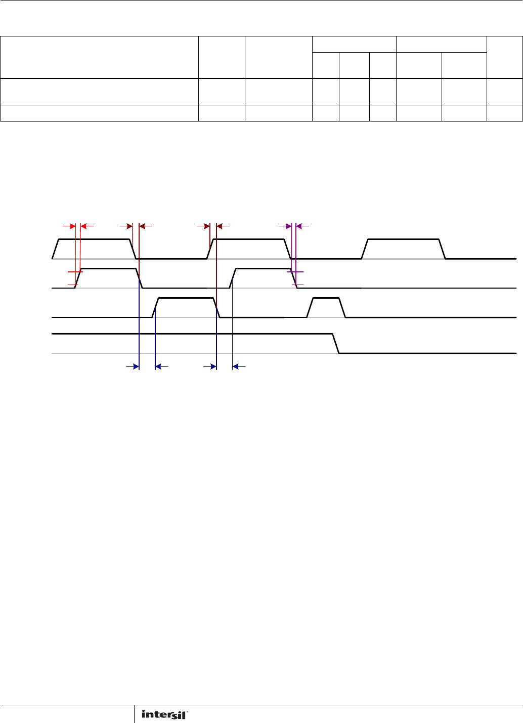
Timing Diagram
Either Output Rise/Fall Time
(3V to 9V/9V to 3V)
t
R,
t
F
C
L
= 0.1mF - 0.5 0.6 - 0.8 µs
Bootstrap Diode Turn-On or Turn-Off Time t
BS
-10- - - ns
NOTES:
9. Parameters with MIN and/or MAX limits are 100% tested at +25°C, unless otherwise specified. Temperature limits are established by
characterization and are not production tested.
10. Dead-Time is defined as the period of time between the LO falling and HO rising or between HO falling and LO rising.
Switching Specifications V
DD
= V
HB
= 12V, V
SS
= V
HS
= 0V, RDT = 0k, No Load on LO or HO, Unless Otherwise Specified. Boldface
limits apply over the operating temperature range, -40°C to +125°C. (Continued)
PARAMETERS SYMBOL
TEST
CONDITIONS
T
J
= +25°C T
J
= -40°C to +125°C
UNITSMIN TYPE MAX
MIN
(Note 9)
MAX
(Note 9)
PWM
HO
LO
EN
t
PLHO
t
PLLO
t
DTLH
t
DTHL
t
R
90%
10%
t
F
90%
10%