HIP2120, HIP2121
11
FN7668.0
December 23, 2011
Functional Description
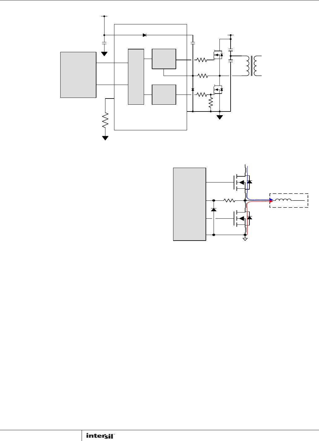
Functional Overview
When connected to a half bridge, the output of the bridge on the
HS node follows the PWM input. In other words, when the PWM
input is high, the high-side bridge FET is turned on and the
low-side FET is off. When the PWM input is low, the low-side
bridge FET is turned on and the high-side is turned off. The
enable pin (EN), when low, drives both outputs to a low state.
When the PWM input transitions high or low, it is necessary to
insure that both bridge FETS are not on at the same time to
prevent shoot-through currents (break before make). The internal
programmable timers delay the rising edge of either output
resulting with both outputs being off before either of the bridge
FETs is driven on. An 8k resistor connected between R
DT
and
VSS results in a nominal dead time of 220ns. An 80k results
with a minimum nominal dead time of 25ns. Resistors values
less than 8k and greater than 80k are not recommended.
The high-side driver bias is established by the boot capacitor
connected between HB and HS. The charge on the boot capacitor
is provided by the internal boot diode that is connected to VDD.
The current path to charge the boot capacitor occurs when the
low-side bridge FET is on. This charge current is limited in
amplitude by the inherent resistance of the boot diode and by the
drain-source voltage of the low-side FET. Assuming that the on
time of the low-side FET is sufficiently long to fully charge the
boot capacitor, the boot voltage will charge very close to VDD
(less the boot diode drop and the low-side FET on voltage).
When the PWM input transitions high, the high-side bridge FET is
driven on after the dead time. Because the HS node is connected
to the source of the high-side FET, the HS node will rise almost to
the level of the bridge voltage (less the conduction voltage across
the bridge FET). Because the boot capacitor voltage is referenced
to the source voltage of the high-side FET, the HB node is V
DD
volts above the HS node and the boot diode is reversed biased.
Because the high-side driver circuit is referenced to the HS node,
the HO output is now approximately VHB + VBRIDGE above
ground.
During the low to high transition of the HS node, the boot
capacitor sources the necessary gate charge to fully enhance the
high-side bridge FET gate. After the gate is fully charged, the boot
capacitor no longer sources the charge to the gate but continues
to provide bias current to the high-side driver. It is clear that the
charge of the boot capacitor must be substantially larger than
the required charge of the high-side FET and high-side driver
otherwise the boot voltage will sag excessively. If the boot
capacitor value is too small for the required maximum of on-time
of the high-side FET, the high-side UV lockout may engage
resulting with an unexpected operation.
Application Information
Selecting the Boot Capacitor Value
The boot capacitor value is chosen not only to supply the internal
bias current of the high-side driver but also, and more
significantly, to provide the gate charge of the driven FET without
causing the boot voltage to sag excessively. In practice, the boot
capacitor should have a total charge that is about 20 times the
gate charge of the driven power FET for approximately a 5% drop
in voltage after the charge has been transferred from the boot
capacitor to the gate capacitance.
The following parameters are required to calculate the value of
the boot capacitor for a specific amount of voltage droop. In this
example, the values used are arbitrary. They should be changed
to comply with the actual application.
The following equations calculate the total charge required for
the Period. This equation assumes that all of the parameters are
constant during the period duration. The error is insignificant if
the ripple is small.
Q
c
= Q
gate80V
+ Period x (I
HB
+ V
HO
/R
GS
+ I
gate_leak
)
C
boot
= Q
c
/(Ripple * VDD)
C
boot
= 0.52µF
If the gate to source resistor is removed (R
GS
is usually not needed
or recommended), then:
C
boot
= 0.33µF
V
DD
= 10V V
DD
can be any value between 7 and 14VDC
V
HB
= V
DD
- 0.6V
= V
HO
High side driver bias voltage (V
DD
- boot diode
voltage) referenced to V
HS
Period = 1ms This is the longest expected switching period
I
HB
= 100µA Worst case high side driver current when
xHO = high
(this value is specified for V
DD
= 12V but the
error is not significant)
R
GS
= 100k Gate-source resistor
(usually not needed)
Ripple= 5% Desired ripple voltage on the boot cap (larger
ripple is not recommended)
I
gate_leak
= 100nA From the FET vendor’s datasheet
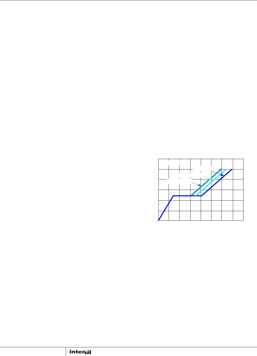
Qgate80V = 64nC From Figure 21
FIGURE 21. TYPICAL GATE CHARGE OF A POWER FET
12
10
8
6
4
2
0
10 20 30 40 50 60 70 80
QG TOTAL GATE CHARGE (nC)
VGS, GATE-TO-SOURCE VOLTAGE (V)
0
V
DS
= 80V
V
DS
= 50V
V
DS
= 20V
I
D
= 33A