19-3443; Rev 3; 4/10
1V to 13.2V, n-Channel Hot-Swap Controllers
Require No Sense Resistor
N
MAX5925
MAX5926
SC_DET
GND
V
CC
REMOVABLE CARD
2.25V TO 13.2V
BACKPLANE
CB SENSEGATE
GND
V
S
1V TO V
CC
V
CC
OUT
R
SC
R
CB
V
OUT
SEE FIGURE 1 FOR A DETAILED TYPICAL OPERATING CIRCUIT WITHOUT R
SENSE
.
TYPICAL OPERATION WITHOUT R
SENSE
General Description
The MAX5924/MAX5925/MAX5926 1V to 13.2V hot-swap
controllers allow the safe insertion and removal of circuit
cards into live backplanes. These devices hot swap sup-
plies ranging from 1V to 13.2V provided that the device
supply voltage, V
CC
, is at or above 2.25V and the hot-
swapped supply, V
S
, does not exceed V
CC
.
The MAX5924/MAX5925/MAX5926 hot-swap controllers
limit the inrush current to the load and provide a circuit-
breaker function for overcurrent protection. The devices
operate with or without a sense resistor. When operat-
ing without a sense resistor, load-probing circuitry
ensures a short circuit is not present during startup,
then gradually turns on the external MOSFET. After the
load probing is complete, on-chip comparators provide
overcurrent protection by monitoring the voltage drop
across the external MOSFET on-resistance. In the event
of a fault condition, the load is disconnected.
The MAX5924/MAX5925/MAX5926 include many inte-
grated features that reduce component count and
design time, including configurable turn-on voltage,
slew rate, and circuit-breaker threshold. An on-board
charge pump provides the gate drive for a low-cost,
external n-channel MOSFET.
The MAX5924/MAX5925/MAX5926 are available with
open-drain PGOOD and/or PGOOD outputs. The
MAX5925/MAX5926 also feature a circuit breaker with
temperature-compensated R
DS(ON)
sensing. The
MAX5926 features a selectable 0ppm/°C or 3300ppm/°C
temperature coefficient. The MAX5924 temperature coef-
ficient is 0ppm/°C and the MAX5925 temperature coeffi-
cient is 3300ppm/°C. Autoretry and latched fault-
management configurations are available (see the
Selector Guide
).
Applications
Base Stations
RAID
Remote-Access Servers
Network Routers and Switches
Servers
Portable Device Bays
Features
o Hot Swap 1V to 13.2V with V
CC
≥ 2.25V
o Drive High-Side n-Channel MOSFET
o Operation With or Without R
SENSE
o Temperature-Compensated R
DS(ON)
Sensing
o Protected During Turn-On into Shorted Load
o Adjustable Circuit-Breaker Threshold
o Programmable Slew-Rate Control
o Programmable Turn-On Voltage
o Autoretry or Latched Fault Management
o 10-Pin µMAX
®
or 16-Pin QSOP Packages
MAX5924/MAX5925/MAX5926
________________________________________________________________
Maxim Integrated Products
1
For pricing, delivery, and ordering information, please contact Maxim Direct at 1-888-629-4642,
or visit Maxim’s website at www.maxim-ic.com.
Typical Operating Circuits
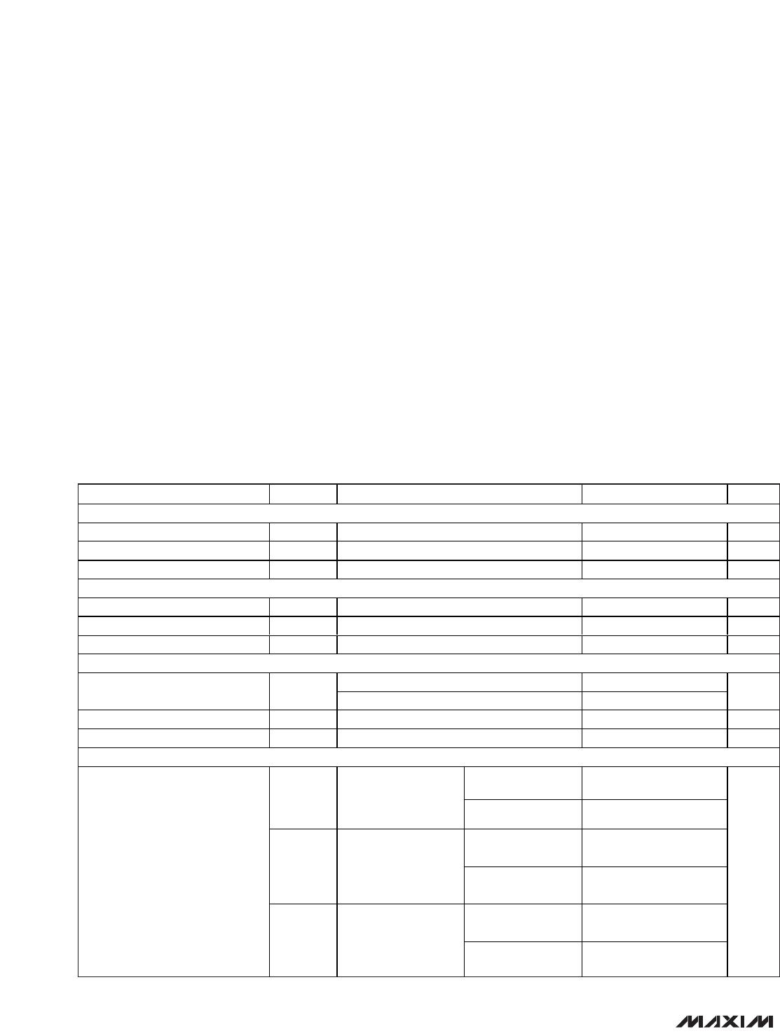
Ordering Information
EVALUATION KIT
AVAILABLE
Selector Guide appears at end of data sheet.
Pin Configurations appear at end of data sheet.
PART TEMP RANGE PIN-PACKAGE
MAX5924AEUB -40°C to +85°C 10 µMAX
MAX5924BEUB -40°C to +85°C 10 µMAX
MAX5924CEUB* -40°C to +85°C 10 µMAX
MAX5924DEUB* -40°C to +85°C 10 µMAX
MAX5925AEUB -40°C to +85°C 10 µMAX
MAX5925BEUB* -40°C to +85°C 10 µMAX
MAX5925CEUB* -40°C to +85°C 10 µMAX
MAX5925DEUB* -40°C to +85°C 10 µMAX
MAX5926EEE -40°C to +85°C 16 QSOP–EP**
Typical Operating Circuits continued at end of data sheet.
*
Future product—contact factory for availability.
**
EP = Exposed pad.
µMAX is a registered trademark of Maxim Integrated Products, Inc.
MAX5924/MAX5925/MAX5926
1V to 13.2V, n-Channel Hot-Swap Controllers
Require No Sense Resistor
2 _______________________________________________________________________________________
ABSOLUTE MAXIMUM RATINGS
ELECTRICAL CHARACTERISTICS
(V
CC
, EN (MAX5924/MAX5925), EN1 (MAX5926) = +2.7V to +13.2V; EN2 (MAX5926) = 0V; V
S
(see Figure 1) = +1.05V to V
CC
;
T
A
= -40°C to +85°C, unless otherwise noted. Typical values are at V
CC
= 5V, R
L
= 500 from OUT to GND, C
L
= 1µF, SLEW =
open, T
A
= +25°C, unless otherwise noted.) (Note 1)
Stresses beyond those listed under “Absolute Maximum Ratings” may cause permanent damage to the device. These are stress ratings only, and functional
operation of the device at these or any other conditions beyond those indicated in the operational sections of the specifications is not implied. Exposure to
absolute maximum rating conditions for extended periods may affect device reliability.
(All voltages referenced to GND, unless otherwise noted.)
V
CC
.........................................................................-0.3V to +14V
GATE*.....................................................................-0.3V to +20V
All Other Pins ............-0.3V to the lower of (V
CC
+ 0.3V) or +14V
SC_DET Current (200ms pulse width, 15% duty cycle) ...140mA
Continuous Current (all other pins) .....................................20mA
Continuous Power Dissipation (T
A
= +70°C)
10-Pin µMAX (derate 6.9mW/°C above +70°C) ...........556mW
16-Pin QSOP (derate 18.9mW/°C above +70°C).......1509mW
Operating Temperature Range ...........................-40°C to +85°C
Junction Temperature .....................................................+150°C
Storage Temperature Range .............................-65°C to +150°C
Lead Temperature (soldering, 10s) .................................+300°C
Soldering Temperature (reflow) .......................................+260°C
PARAMETER SYMBOL CONDITIONS MIN TYP MAX UNITS
POWER SUPPLIES
V
CC
Operating Range V
CC
2.7 13.2 V
V
S
Operating Range V
S
V
S
as defined in Figure 1 1.0 V
CC
V
Supply Current I
CC
FET is fully enhanced, SC_DET = V
CC
1.5 2.5 mA
UNDERVOLTAGE LOCKOUT (UVLO)
UVLO Threshold V
UVLO
D efaul t val ue, V
S
and V
C C
i ncr easi ng , Fi g ur e 1 1.73 2.06 2.47 V
V
CC
UVLO Deglitch Time t
DG
(Note 2) 900 µs
V
CC
UVLO Startup Delay t
D
,
UVLO
123 200 350 ms
LOAD-PROBE
2.7V < V
CC
< 5V 4 30 65
Load-Probe Resistance (Note 3) R
LP
5V < V
CC
< 13.2V 3 10 20
Load-Probe Timeout t
LP
43 102 205 ms
Load-Probe Threshold Voltage V
LP,TH
(Note 4) 172 200 235 mV
CIRCUIT BREAKER
V
CC
= 2.7V and V
CB
= 1V
37
I
CB
TC = high
(MAX5926), MAX5924
2.7V V
CC
13.2V 34 37 42
V
CC
= 2.7V, V
CB
=
1V, T
A
= +25°C
30 40 50
I
CB25
TC = low (MAX5926),
MAX5925 (Note 5)
2.7V V
CC
13.2V,
T
A
= +25°C
40 50 60
V
CC
= 2.7V and V
CB
= 1V, T
A
= +85°C
40 50 60
Circuit-Breaker Programming
Current
I
CB85
TC = low (MAX5926),
MAX5925 (Note 5)
2.7V V
CC
13.2V,
T
A
= +85°C
50 60 70
µA
*
GATE is internally driven and clamped. Do not drive GATE with external source.
MAX5924/MAX5925/MAX5926
1V to 13.2V, n-Channel Hot-Swap Controllers
Require No Sense Resistor
_______________________________________________________________________________________ 3
ELECTRICAL CHARACTERISTICS (continued)
(V
CC
, EN (MAX5924/MAX5925), EN1 (MAX5926) = +2.7V to +13.2V; EN2 (MAX5926) = 0V; V
S
(see Figure 1) = +1.05V to V
CC
;
T
A
= -40°C to +85°C, unless otherwise noted. Typical values are at V
CC
= 5V, R
L
= 500 from OUT to GND, C
L
= 1µF, SLEW =
open, T
A
= +25°C, unless otherwise noted.) (Note 1)
PARAMETER SYMBOL CONDITIONS MIN TYP MAX UNITS
Circuit-Breaker Programming
Current During Startup
I
CB,SU
2 x I
CB
µA
Circuit-Breaker Enable Threshold V
CB
,
EN
V
GATE
- V
OUT
, rising gate voltage (Note 6) 2.3 3.6 4.65 V
Circuit-Breaker Comparator Offset
Voltage
V
CB_OS
0.3 ±4.7 mV
Fast Circuit-Breaker Offset
Resistor
R
CBF
Figure 3 1.2 1.9 2.7 k
Slow Circuit-Breaker Delay t
CBS
V
CB
- V
SENSE
= 10mV 0.95 1.6 2.95 ms
Fast Circuit-Breaker Delay t
CBF
V
CB
- V
SENSE
= 500mV 280 ns
Circuit-Breaker Trip Gate
Pulldown Current
I
GATE
,
PD
V
GATE
= 2.5V, V
CC
= 13.2V 13.5 27 mA
MAX5924, TC = high (MAX5926) 0
Circuit-Breaker Temperature
Coefficient
TC
ICB
MAX5925, TC = low (MAX5926) 3300
ppm/°C
OUT Current I
OUT
120 µA
MOSFET DRIVER
External Gate Drive V
GS
V
GATE
- V
OUT
2.7V V
CC
13.2V 4.2 5.5 7.2 V
SLEW = open, C
GATE
= 10nF 2.19 9.5
Load Voltage Slew Rate SR
C
SLEW
= 300nF, C
GATE
= 10nF (Note 8) 0.84
V/ms
Gate Pullup Current Capacity I
GATE
V
GATE
= 0V 239 µA
ENABLE COMPARATOR
EN, EN1 Reference Threshold V
EN/UVLO
V
EN
(MAX5924/MAX5925) or
V
EN1
(MAX5926) rising
0.747 0.795 0.850 V
EN, EN1 Hysteresis V
EN
,
HYS
30 mV
EN, EN1 Input Bias Current I
EN
EN (MAX5924/MAX5925) = V
CC
,
EN1 (MAX5926) = V
CC
±8 ±50 nA
DIGITAL OUTPUTS (PGOOD, PGOOD)
Power-Good Output Low Voltage V
OL
I
OL
= 1mA 0.3 0.4 V
Power-Good Output Open-Drain
Leakage Current
I
OH
PGOOD/PGOOD = 13.2V 0.2 1 µA
Power-Good Trip Point V
THPGOOD
V
GATE
- V
OUT
, rising gate voltage V
CB
_
EN
3.6 4.7 V
Power-Good Hysteresis V
PG
,
HYS
0.36 V

MAX5924BEUB+

Mfr. #:
Manufacturer:
Maxim Integrated
Description:
Hot Swap Voltage Controllers 1-13.2V Hot-Swap Controller
Lifecycle:
New from this manufacturer.
Delivery:
DHL FedEx Ups TNT EMS
Payment:
T/T Paypal Visa MoneyGram Western Union