MAX5924/MAX5925/MAX5926
1V to 13.2V, n-Channel Hot-Swap Controllers
Require No Sense Resistor
______________________________________________________________________________________ 13
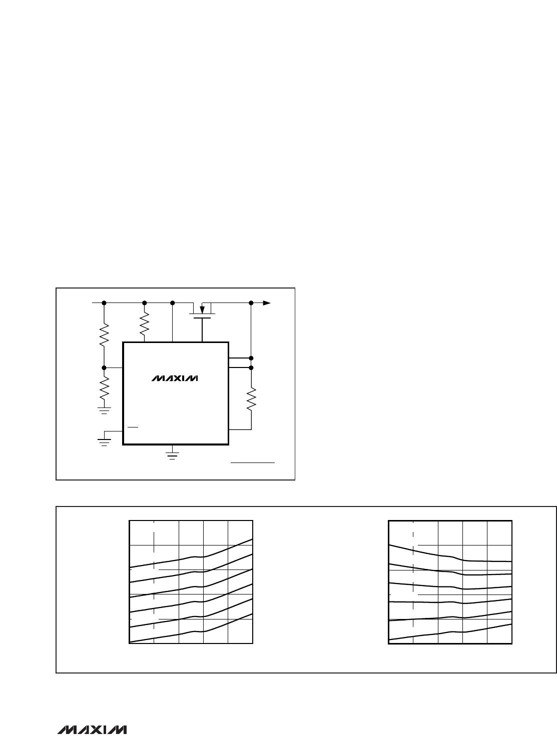
Bilevel Fault Protection
Bilevel Fault Protection in Startup Mode
Bilevel fault protection is disabled in startup mode, and
is enabled when V
GATE-VOUT
exceeds V
CB,EN
at the
end of the startup period.
When no R
SENSE
is detected, neither slow nor fast com-
parator is active during startup because the high
RD(ON) of the MOSFET when not fully enhanced would
signal an artificially-high V
IN
-V
SENSE
voltage. Load prob-
ing prior to startup insures that the output is not short cir-
cuited.
When R
SENSE
is detected, the slow comparator is dis-
abled during startup while the fast comparator remains
active. The overcurrent trip level is higher than normal
during the startup period because the ICB is temporarily
doubled to ICB,SU at this time. This allows higher than
normal startup current to allow for output capacitor
charging current.
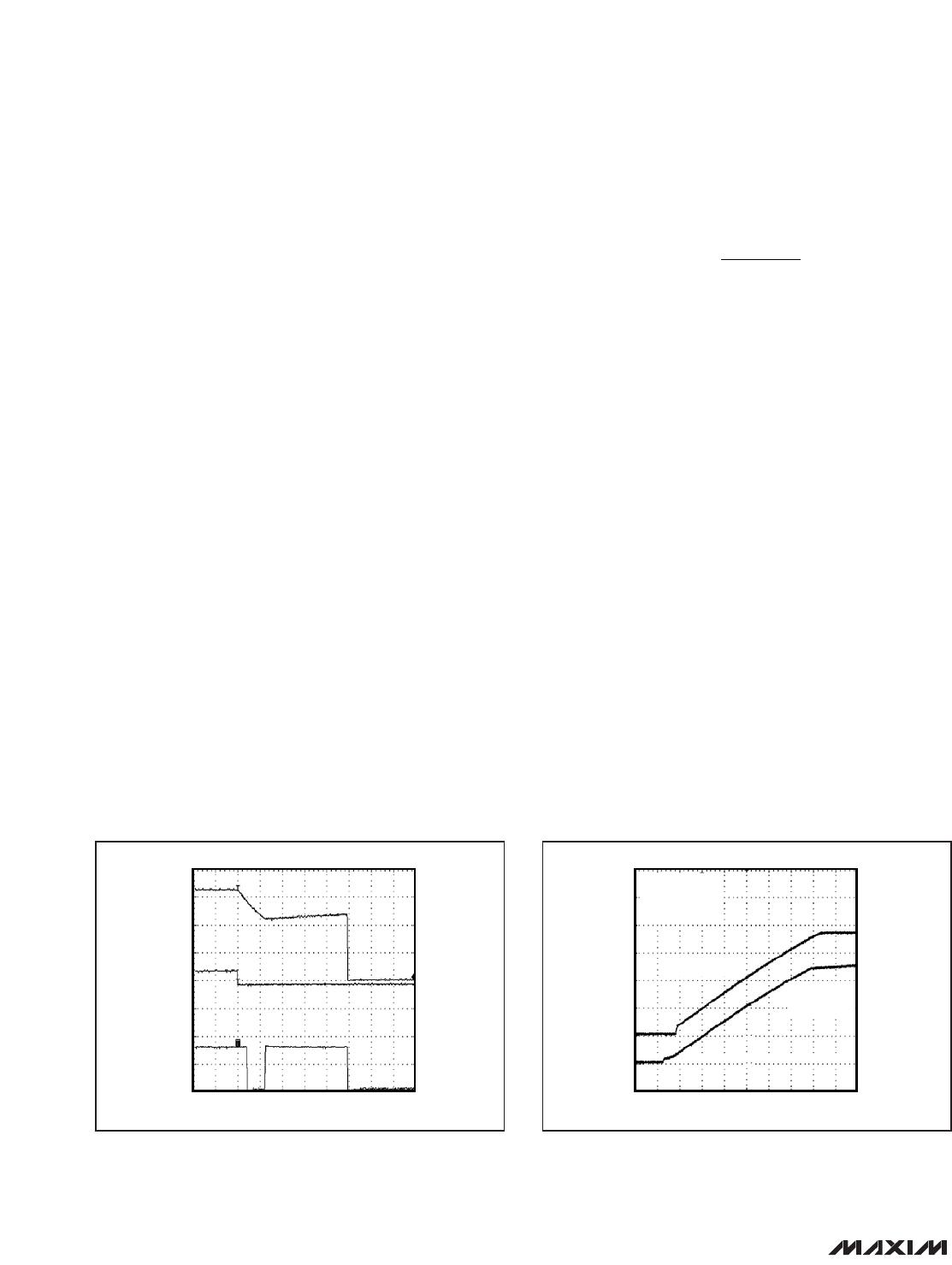
Slow Comparator
The slow comparator is disabled during startup while
the external MOSFET turns on.
If the slow comparator detects an overload condition while
in normal operation (after startup is complete), it turns off
the external MOSFET by discharging the gate capaci-
tance with I
GATE,PD
. The magnitude of I
GATE,PD
depends on the external MOSFET gate-to-source volt-
age, V
GS
. The discharge current is strongest immedi-
ately following a fault and decreases as the MOSFET
gate is discharged (Figure 8a).
Fast Comparator
The fast comparator is used for serious current overloads
or short circuits. If the load current reaches the fast com-
parator threshold, the device quickly forces the MOSFET
off. The fast comparator has a response time of 280ns,
and discharges GATE with I
GATE,PD
(Figure 8a). The fast
comparator is disabled during startup when no R
SENSE
is detected
Latched and Autoretry Fault Management
The MAX5924A, MAX5924B, MAX5925A, and MAX5925B
latch the external MOSFET off when an overcurrent fault
is detected. Following an overcurrent fault, the
MAX5924C, MAX5924D, MAX5925C, and MAX5925D
enter autoretry mode. The MAX5926 can be configured
for either latched or autoretry mode (see Table 1).
In autoretry, a fault turns the external MOSFET off then
automatically restarts the device after the autoretry
delay, t
RETRY
. During the autoretry delay, pull EN or
EN1 low to restart the device. In latched mode, pull EN
or EN1 low for at least 100µs to clear a latched fault
and restart the device.
Power-Good Outputs
The power-good output(s) are open-drain output(s) that
deassert:
• When V
CC
< V
UVLO
• During t
D,UVLO
• When V
GS
< V
THPGOOD
• During load probing
• When disabled (EN = GND (MAX5924/MAX5925),
EN1 = GND or EN2 = high (MAX5926))
• During fault management
• During t
RETRY
or when latched off (MAX5924A,
MAX5924B, MAX5925A, MAX5925B, or MAX5926
(LATCH = low)).
PGOOD/PGOOD asserts only if the part is in normal
mode and no faults are present.