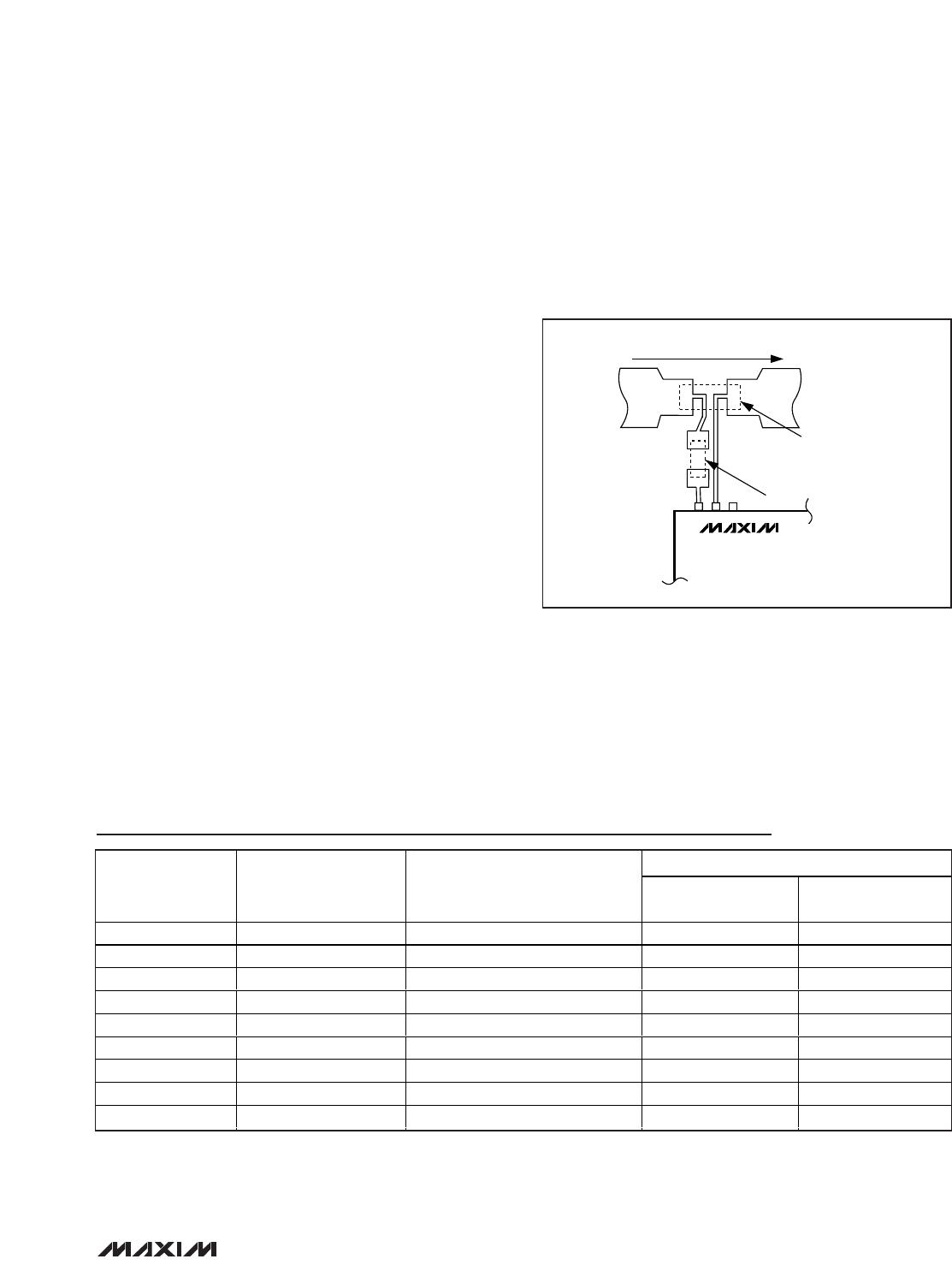
Layout Considerations
Keep all traces as short as possible and maximize the
high-current trace dimensions to reduce the effect of
undesirable parasitic inductance. Place the MAX5924/
MAX5925/MAX5926 close to the card’s connector. Use
a ground plane to minimize impedance and induc-
tance. Minimize the current-sense resistor trace length
(<10mm), and ensure accurate current sensing with
Kelvin connections.
When the output is short circuited, the voltage drop
across the external MOSFET becomes large. Hence, the
power dissipation across the switch increases, as does
the die temperature. An efficient way to achieve good
power dissipation on a surface-mount package is to lay
out two copper pads directly under the MOSFET pack-
age on both sides of the board. Connect the two pads
to the ground plane through vias, and use enlarged
copper mounting pads on the top side of the board.
It is important to maximize the thermal coupling between
the MOSFET and the MAX5925/MAX5926 to balance the
device junction temperatures. When the temperatures of
the two devices are equal, the circuit-breaker trip
threshold is most accurate. Keep the MOSFET and the
MAX5925/MAX5926 as close to each other as possible
to facilitate thermal coupling.
MAX5924/MAX5925/MAX5926
1V to 13.2V, n-Channel Hot-Swap Controllers
Require No Sense Resistor
______________________________________________________________________________________ 19