PDF: 09005aef81c9620b/Source: 09005aef81c961ec Micron Technology, Inc., reserves the right to change products or specifications without notice.
HVF9C64_128x72K.fm - Rev. C 3/07 EN
4 ©2005 Micron Technology, Inc. All rights reserved.
512MB, 1GB: (x72, ECC, SR) 244-Pin DDR2 VLP Mini-RDIMM
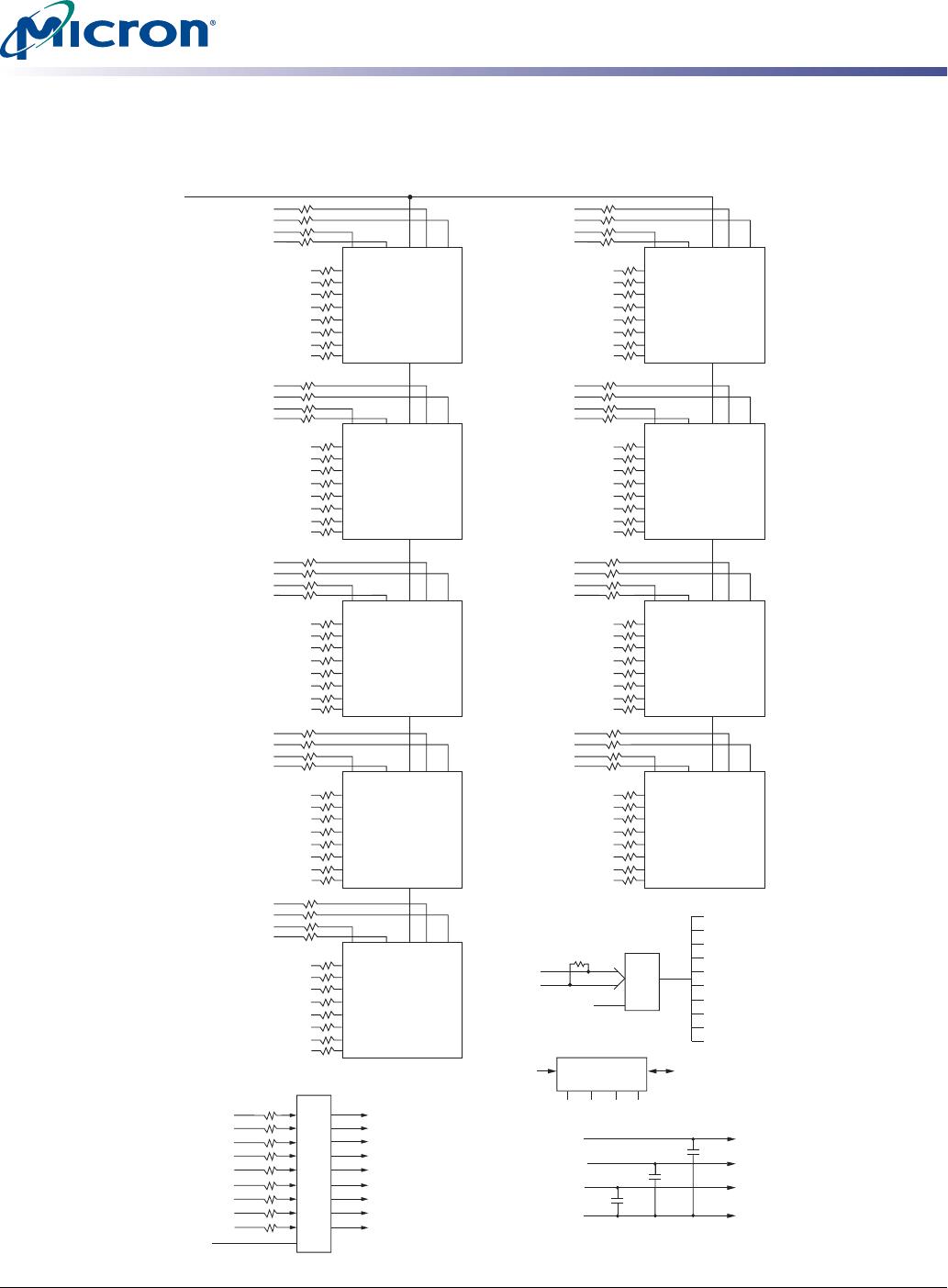
Pin Assignments and Descriptions
Table 6: Pin Descriptions
Symbol Type Description
ODT0 Input
(SSTL_18)
On-die termination: ODT (registered HIGH) enables termination resistance internal to
the DDR2 SDRAM. When enabled, ODT is only applied to each of the following pins: DQ,
DQS, DQS#, RDQS, RDQS#, CB, and DM. The ODT input will be ignored if disabled via the
LOAD MODE (LM) command.
CK0, CK0# Input
(SSTL_18)
Clock: CK and CK# are differential clock inputs. All address and control input signals are
sampled on the crossing of the positive edge of CK and negative edge of CK#. Output data
(DQs and DQS/DQS#) is referenced to the crossings of CK and CK#.
CKE0 Input
(SSTL_18)
Clock enable: CKE (registered HIGH) activates and CKE (registered LOW) deactivates
clocking circuitry on the DDR2 SDRAM.
S0# Input
(SSTL_18)
Chip select: S# enables (registered LOW) and disables (registered HIGH) the command
decoder. All commands are masked when S# is registered HIGH. S# provides for external
rank selection on systems with multiple ranks. S# is considered part of the command code.
RAS#, CAS#, WE# Input
(SSTL_18)
Command inputs: RAS#, CAS#, and WE# (along with S#) define the command being
entered.
BA0, BA1
(512MB)
BA0–BA2
(1GB)
Input
(SSTL_18)
Bank address inputs: BA0–BA1/BA2 define to which device bank an ACTIVE, READ,
WRITE, or PRECHARGE command is being applied. BA0–BA1/BA2 define which mode
register, including MR, EMR, EMR(2), and EMR(3), is loaded during the LM command.
A0–A13 Input
(SSTL_18)
Address inputs: Provide the row address for ACTIVE commands, and the column address
and auto precharge bit (A10) for READ/WRITE commands, to select one location out of the
memory array in the respective bank. A10 sampled during a PRECHARGE command
determines whether the PRECHARGE applies to one device bank (A10 LOW, device bank
selected by BA0–BA1/BA2) or all device banks (A10 HIGH). The address inputs also provide
the op-code during a LM command.
P
AR_IN Input
(SSTL_18)
Parity bit for the address and control bus.
SCL Input
(SSTL_18)
Serial clock for presence-detect: SCL is used to synchronize the presence-detect data
transfer to and from the module.
SA0–SA2 Input
(SSTL_18)
Presence-detect address inputs: These pins are used to configure the presence-detect
device.
RESET# Input
(SSTL_18)
Asynchronously forces all registered outputs LOW when RESET# is LOW. This signal can be
used during power-up to ensure that CKE is LOW and DQs are High-Z.
DQ0–DQ63 I/O
(SSTL_18)
Data input/output: Bidirectional data bus.
DQS0–DQS8,
DQS0#–DQS8#
I/O
(SSTL_18)
Data strobe: Output with read data, input with write data for source synchronous
operation. Edge-aligned with read data, center-aligned with write data. DQS# is only used
when differential data strobe mode is enabled via the LM command. DQS9#–DQS17# are
only used when RDQS# is enabled via the LM command.
DM0–DM8
(RDQS0–RDQS8)
I/O
(SSTL_18)
Input data mask: DM is an input mask signal for write data. Input data is masked when
DM is sampled HIGH along with that input data during a WRITE access. DM is sampled on
both edges of DQS. Although DM pins are input-only, the DM loading is designed to match
that of DQ and DQS pins. If RDQS is enabled, DQS0#–DQS8# are used only during the READ
command. If RDQS is disabled, RDQS0–RDQS8 become DM0–DM8 and RDQS0#–RDQS8# are
not used.
CB0–CB7 I/O
(SSTL_18)
Check bits.
SDA I/O
(SSTL_18)
Serial presence-detect data: SDA is a bidirectional pin used to transfer addresses and
data into and out of the presence-detect portion of the module.
E
RR_OUT Output
(open drain)
Parity error found on the address and control bus.
V
DD/VDDQ Supply
Power supply: 1.8V ±0.1V.