DS3234
Extremely Accurate SPI Bus RTC with
Integrated Crystal and SRAM
4 _____________________________________________________________________
AC ELECTRICAL CHARACTERISTICS
(V
CC
= 2.0V to 5.5V, T
A
= -40°C to +85°C, unless otherwise noted.) (Note 2)
PARAMETER SYMBOL CONDITIONS MIN TYP MAX UNITS
2.7V V
CC
5.5V 4
SCLK Clock Frequency f
SCL
2.0V V
CC
< 2.7V 2
MHz
Data to SCLK Setup t
DC
30 ns
SCLK to Data Hold t
CDH
30 ns
SCLK to CS Setup t
CCS
30 ns
2.7V V
CC
5.5V 80
SCLK to Data Valid (Note 7) t
CDD
2.0V V
CC
< 2.7V 160
ns
2.7V V
CC
5.5V 110
SCLK Low Time t
CL
2.0V V
CC
< 2.7V 220
ns
2.7V V
CC
5.5V 110
SCLK High Time t
CH
2.0V V
CC
< 2.7V 220
ns
SCLK Rise and Fall t
R
, t
F
200 ns
CS to SCLK Setup t
CC
400 ns
2.7V V
CC
5.5V 100
SCLK to CS Hold t
CCH
2.0V V
CC
< 2.7V 200
ns
CS Inactive Time t
CWH
400 ns
CS to Output High Impedance t
CDZ
(Note 8) 40 ns
Pushbutton Debounce PBDB 250 ms
Reset Active Time t
RST
250 ms
Oscillator Stop Flag (OSF) Delay t
OSF
(Note 9) 100 ms
Temperature Conversion Time t
CONV
125 200 ms
POWER-SWITCH CHARACTERISTICS
(T
A
= -40°C to +85°C)
PARAMETER SYMBOL CONDITIONS MIN TYP MAX UNITS
V
CC
Fall Time; V
PF(MAX)
to
V
PF(MIN)
t
VCCF
300 µs
V
CC
Rise Time; V
PF(MIN)
to
V
PF(MAX)
t
VCCR
s
Recovery at Power-Up t
REC
(Note 10) 125 300 ms
CAPACITANCE
(T
A
= +25°C)
PARAMETER SYMBOL CONDITIONS MIN TYP MAX UNITS
Capacitance on All Input Pins C
IN
(Note 11) 10 pF
Capacitance on All Output Pins C
IO
Outputs high impedance (Note 11) 10 pF
DS3234
Extremely Accurate SPI Bus RTC with
Integrated Crystal and SRAM
_____________________________________________________________________ 5
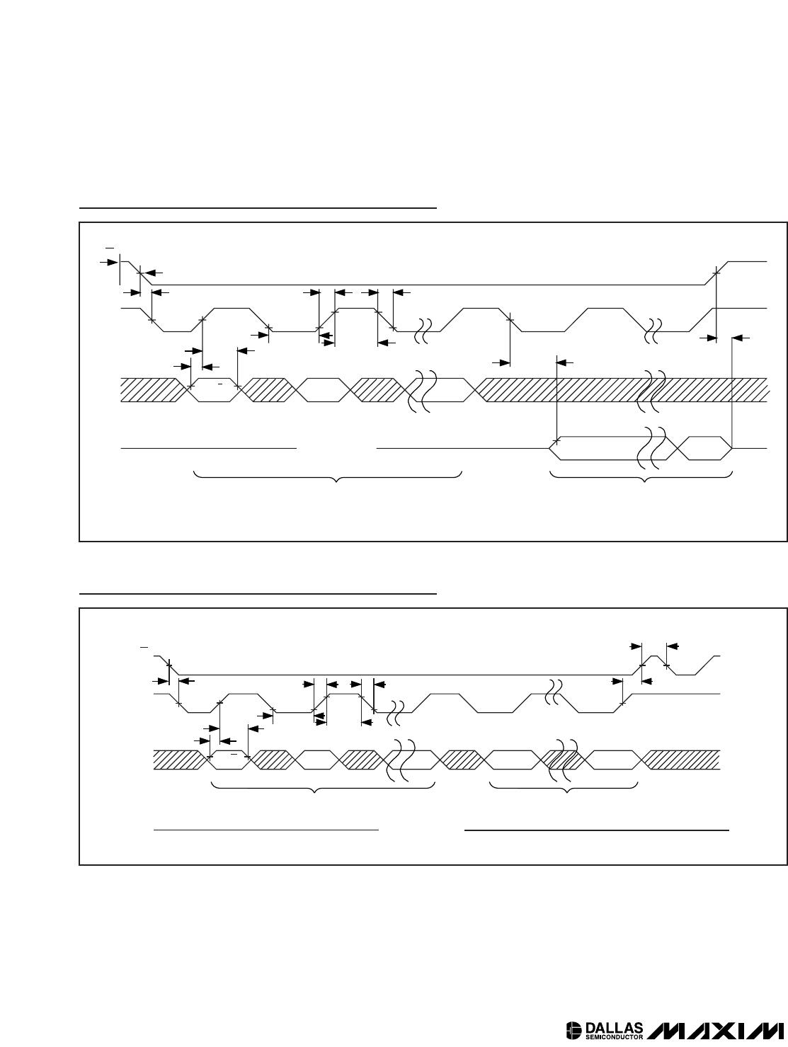
Pushbutton Reset Timing
t
RST
PB
DB
RST
Power-Switch Timing
V
CC
V
PF(MAX)
RST
V
PF(MIN)
t
VCCF
t
VCCR
t
REC
V
PF
V
PF
Note 2: Limits at -40°C are guaranteed by design and not production tested.
Note 3: All voltages are referenced to ground.
Note 4: Measured at V
IH
= 0.8 x V
CC
or V
IL
= 0.2 x V
CC
, 10ns rise/fall time, DOUT = no load.
Note 5: Current is the averaged input current, which includes the temperature conversion current. CRATE1 = CRATE0 = 0.
Note 6: The RST pin has an internal 50kΩ (nominal) pullup resistor to V
CC
.
Note 7: Measured at V
OH
= 0.8 x V
CC
or V
OL
= 0.2 x V
CC
. Measured from the 50% point of SCLK to the V
OH
minimum of DOUT.
Note 8: With 50pF load.
Note 9: The parameter t
OSF
is the period of time the oscillator must be stopped for the OSF flag to be set over the voltage range of
0V V
CC
V
CC(MAX)
and 2.3V V
BAT
V
BAT(MAX)
.
Note 10: This delay only applies if the oscillator is enabled and running. If the EOSC bit is 1, t
REC
is bypassed and RST immediately
goes high.
Note 11: Guaranteed by design and not production tested.
WARNING: Negative undershoots below -0.3V while the part is in battery-backed mode may
cause loss of data.
DS3234
Extremely Accurate SPI Bus RTC with
Integrated Crystal and SRAM
6 _____________________________________________________________________
Timing Diagram—SPI Read Transfer
HIGH IMPEDANCE
CS
SCLK
DIN
W/R
t
DC
t
CL
t
CH
t
CDD
t
CDZ
t
CDH
t
CC
t
CCS
t
R
t
F
A6
A0
D0
WRITE ADDRESS BYTE
NOTE: SCLK CAN BE EITHER POLARITY, SHOWN FOR CPOL = 1.
READ DATA BYTE
DOUT
D7
Timing Diagram—SPI Write Transfer
CS
SCLK
DIN
W/R
t
DC
t
CDH
t
CL
t
CH
t
CCH
t
CWH
t
F
t
R
t
CC
A6
A0
WRITE ADDRESS BYTE
WRITE DATA BYTE
D7 D0
DOUT
HIGH IMPEDANCE

DS3234S#

Mfr. #:
Manufacturer:
Maxim Integrated
Description:
Real Time Clock Integrated RTC/TCXO/Crystal
Lifecycle:
New from this manufacturer.
Delivery:
DHL FedEx Ups TNT EMS
Payment:
T/T Paypal Visa MoneyGram Western Union

Products related to this Datasheet