IDT
®
Nineteen Output Differential Buffer for PCIe Gen3
9DB1933
Nineteen Output Differential Buffer for PCIe Gen3
10
1676A—07/12/10
Common Recommendations for Differential Routing Dimension or Value Unit Figure
L1 length, route as non-coupled 50ohm trace 0.5 max inch 1
L2 length, route as non-coupled 50ohm trace 0.2 max inch 1
L3 length, route as non-coupled 50ohm trace 0.2 max inch 1
Rs 33 ohm 1
Rt 49.9 ohm 1
Down Device Differential Routing
L4 length, route as coupled microstrip 100ohm differential trace 2 min to 16 max inch 1
L4 length, route as coupled stripline 100ohm differential trace 1.8 min to 14.4 max inch 1
Differential Routing to PCI Express Connector
L4 length, route as coupled microstrip 100ohm differential trace 0.25 to 14 max inch 2
L4 length, route as coupled stripline 100ohm differential trace 0.225 min to 12.6 max inch 2
DIF Reference Clock
HCSL Output Buffer
L1
L1'
Rs
L2
L2'
Rs
L4'
L4
L3L3'
Rt Rt
PCI Express
Down Device
REF_CLK Input
Figure 1: Down Device Routing
HCSL Output Buffer
L1
L1'
Rs
L2
L2'
Rs
L4'
L4
L3L3'
Rt Rt
PCI Express
Add-in Board
REF_CLK Input
Figure 2: PCI Express Connector Routing
IDT
®
Nineteen Output Differential Buffer for PCIe Gen3
9DB1933
Nineteen Output Differential Buffer for PCIe Gen3
11
1676A—07/12/10
Vdiff Vp-p Vcm R1 R2 R3 R4 Note
0.45v 0.22v 1.08 33 150 100 100
0.58 0.28 0.6 33 78.7 137 100
0.80 0.40 0.6 33 78.7 none 100 ICS874003i-02 input compatible
0.60 0.3 1.2 33 174 140 100 Standard LVDS
R1a = R1b = R1
R2a = R2b = R2
Alternative Termination for LVDS and other Common Differential Signals (figure 3)
HCSL Output Buffer
L1
L1'
R1b
L2
L2'
R1a
L4'
L4
L3
R2a R2b
Down Device
REF_CLK Input
Figure 3
L3'
R3 R4
PCIe Device
REF_CLK Input
Figure 4
R5a
L4'
L4
3.3 Volts
R5b
R6a R6b
Cc
Cc
Component Value Note
R5a, R5b 8.2K 5%
R6a, R6b 1K 5%
Cc 0.1 µF
Vcm 0.350 volts
Cable Connected AC Coupled Application (figure 4)
IDT
®
Nineteen Output Differential Buffer for PCIe Gen3
9DB1933
Nineteen Output Differential Buffer for PCIe Gen3
12
1676A—07/12/10
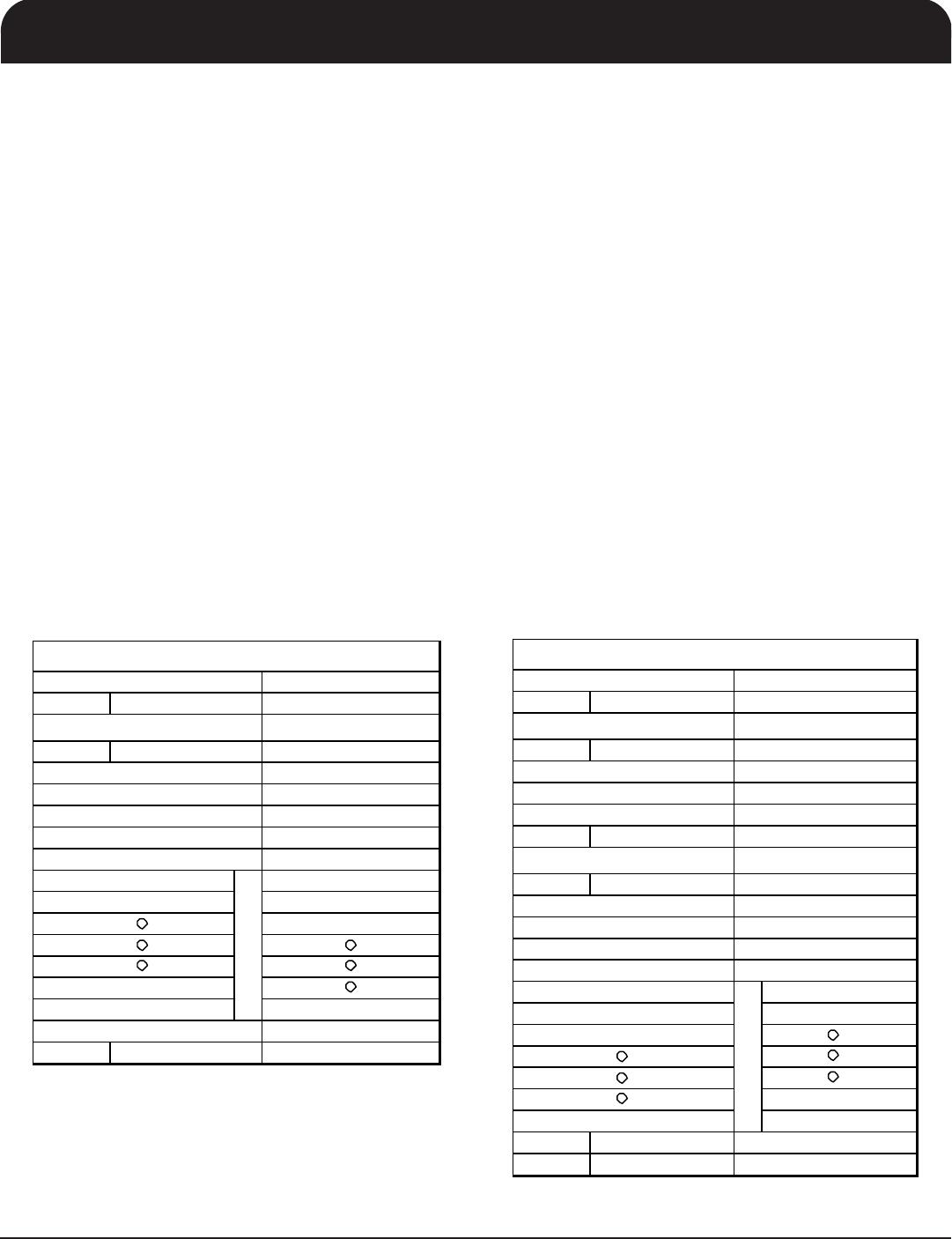
General SMBus serial interface information for the 9DB1933
How to Write:
Controller (host) sends a start bit.
Controller (host) sends the write address DC
(h)
ICS clock will acknowledge
Controller (host) sends the begining byte location = N
ICS clock will acknowledge
Controller (host) sends the data byte count = X
ICS clock will acknowledge
Controller (host) starts sending Byte N through
Byte N + X -1
ICS clock will acknowledge each byte one at a time
Controller (host) sends a Stop bit
How to Read:
Controller (host) will send start bit.
Controller (host) sends the write address DC
(h)
ICS clock will acknowledge
Controller (host) sends the begining byte
location = N
ICS clock will acknowledge
Controller (host) will send a separate start bit.
Controller (host) sends the read address DD
(h)
ICS clock will acknowledge
ICS clock will send the data byte count = X
ICS clock sends Byte N + X -1
ICS clock sends Byte 0 through byte X (if X
(h)
was written to byte 8).
Controller (host) will need to acknowledge each byte
Controllor (host) will send a not acknowledge bit
Controller (host) will send a stop bit
ICS (Slave/Receiver)
T
WR
ACK
ACK
ACK
ACK
ACK
P stoP bit
X Byte
Index Block Write Operation
Slave Address DC
(h)
Beginning Byte = N
WRite
starT bit
Controller (Host)
Byte N + X - 1
Data Byte Count = X
Beginning Byte N
T starT bit
WR WRite
RT Repeat starT
RD ReaD
Beginning Byte N
Byte N + X - 1
N Not acknowledge
P stoP bit
Slave Address DD
(h)
Index Block Read Operation
Slave Address DC
(h)
Beginning Byte = N
ACK
ACK
Data Byte Count = X
ACK
ICS (Slave/Receiver)
Controller (Host)
X Byte
ACK
ACK
Note: Addresses show assumes pin 29 is low.

9DB1933AKLF

Mfr. #:
Manufacturer:
IDT
Description:
Clock Buffer 19 OUTPUT PCIE GEN3 BUFFER
Lifecycle:
New from this manufacturer.
Delivery:
DHL FedEx Ups TNT EMS
Payment:
T/T Paypal Visa MoneyGram Western Union

Products related to this Datasheet