IDT
®
Nineteen Output Differential Buffer for PCIe Gen3
9DB1933
Nineteen Output Differential Buffer for PCIe Gen3
7
1676A—07/12/10
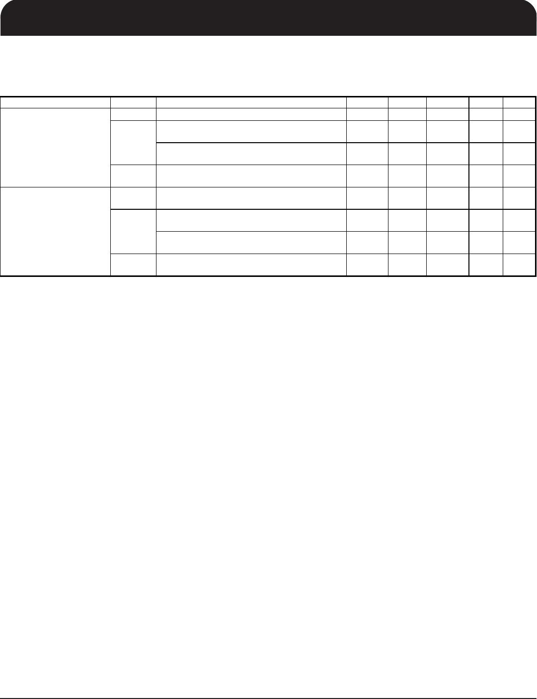
Electrical Characteristics - Output Duty Cycle, Jitter, Skew and PLL Characterisitics
TA = T
COM;
Supply Voltage VDD = 3.3 V +/-5%
PARAMETER SYMBOL CONDITIONS MIN TYP MAX UNITS NOTES
-3dB point in High BW Mode
2
3
4
MHz
1
-3dB point in Low BW Mode
0.7
1
1.4
MHz
1
PLL Jitter Peaking
t
JPEAK
Peak Pass band Gain 1.4 2 dB 1
Duty Cycle
t
DC
Measured differentially, PLL Mode 45 49.5 55 % 1,2
Duty Cycle Distortion
t
DCD
Measured differentially, Bypass Mode @100MHz -2 1 2 % 1,2,5
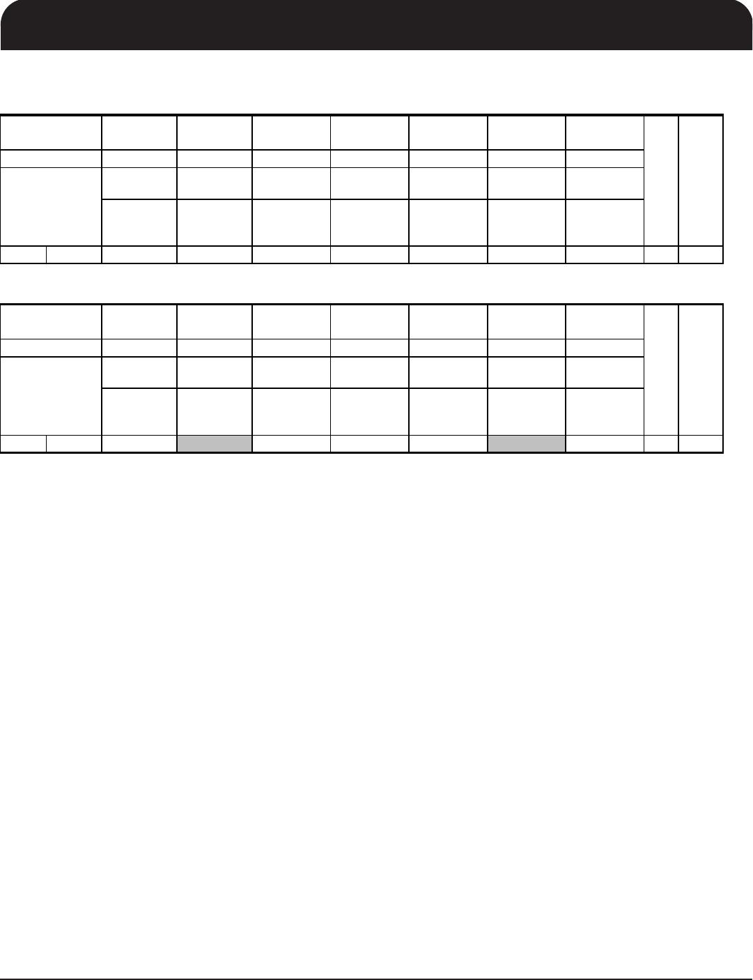
t
pdBYP
Bypass Mode, nominal value @ 25°C, 3.3V,
V
T
= 50%
2500 3700 4500 ps 1,2,4
t
pdPLL
PLL Mode, nominal value @ 25°C, 3.3V,
V
T
= 50%
100 300 500 ps 1,2,3
DIF_IN, DIF [x:0]
t
pd_BYP
Input-to-Output Skew Variation in Bypass mode
(over specified voltage / temperature operating
ranges)
|500| |600| ps
1,2,4,6,
7,8,9,
13
DIF_IN, DIF [x:0]
t
pd_PLL
Input-to-Output Skew Variation in PLL mode
(over specified voltage / temperature operating
ranges)
|250| |350| ps
1,2,3,6,
7,8,9,
13
DIF[X:0]
t
JPH
Differential Phase Jitter (RMS Value) 2 10 ps 1,7,10
DIF[X:0]
t
SSTERROR
Differential Spread Spectrum Tracking Error (peak
to peak)
40 80 ps 1,7,12
Skew, Output to Output
t
sk3
V
T
= 50%
100 150 ps 1
PLL mode
40
50
ps
1,2
Additive Jitter in Bypass Mode 25 50 ps 1,2
1
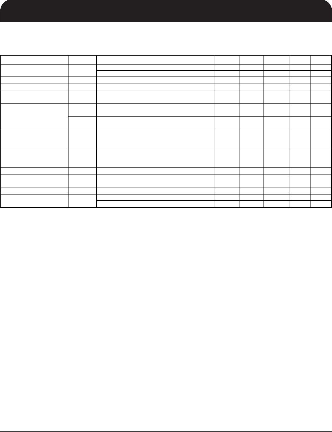
Guaranteed by design and characterization, not 100% tested in production. C
LOAD
= 2pF
5
Duty cycle distortion is the difference in duty cycle between the output and the input clock when the device is operated in bypass mode.
6
VT = 50% of Vout
11
t is the period of the input clock
PLL Bandwidth BW
3
PLL mode Input-to-Output skew is measured at the first output edge following the corresponding input.
2
Measured from differential cross-point to differential cross-point
4
All Bypass Mode Input-to-Output specs refer to the timing between an input edge and the specific output edge created by it.
7
This parameter is deterministic for a given device
13
This parameter is an absolute value. It is not a double-sided figure.
Skew, Input to Output
Jitter, Cycle to cycle
9
Long-term variation from nominal of input-to-output skew over temperature and voltage for a single device.
10
This parameter is measured at the outputs of two separate 9DB1933 devices driven by a single main clock. The 9DB1933's must be
set to high bandwidth. Differential phase jitter is the accumulation of the phase jitter not shared by the outputs (eg. not including the
12
Differential spread spectrum tracking error is the difference in spread spectrum tracking between two 9DB1933 devices This parameter
is measured at the outputs of two separate 9DB1933 devices driven by a single main clock in Spread Spectrum mode. The 9DB1933's
must be set to high bandwidth. The spread spectrum characteristics are: maximum of 0.5%, 30-33KHz modulation frequency, linear
t
jcyc-cyc
8
Measured with scope averaging on to find mean value.
IDT
®
Nineteen Output Differential Buffer for PCIe Gen3
9DB1933
Nineteen Output Differential Buffer for PCIe Gen3
8
1676A—07/12/10
Electrical Characteristics - PCIe Phase Jitter Parameters
TA = T
COM;
Supply Voltage VDD = 3.3 V +/-5%
PARAMETER SYMBOL CONDITIONS MIN TYP MAX UNITS Notes
t
jphPCIeG1
PCIe Gen 1 44 86 ps (p-p) 1,2,3
PCIe Gen 2 Lo Band
10kHz < f < 1.5MHz
1.4 3
ps
(rms)
1,2
PCIe Gen 2 High Band
1.5MHz < f < Nyquist (50MHz)
2.5
3.1
ps
(rms)
1,2
t
jphPCIeG3
PCIe Gen 3
(PLL BW of 2-4MHz, CDR = 10MHz)
0.6
1
ps
(rms)
1,2,4
t
jphPCIeG1
PCIe Gen 1 3 5 ps (p-p) 1,2,3
PCIe Gen 2 Lo Band
10kHz < f < 1.5MHz
0.02 0.1
ps
(rms)
1,2
PCIe Gen 2 High Band
1.5MHz < f < Nyquist (50MHz)
0.2
0.3
ps
(rms)
1,2
t
jphPCIeG3
PCIe Gen 3
(PLL BW of 2-4MHz, CDR = 10MHz)
0.04
0.1
ps
(rms)
1,2,4
1
Applies to all outputs.
4
Subject to final radification by PCI SIG.
t
jphPCIeG2
2
See http://www.pcisig.com for complete specs
t
jphPCIeG2
Phase Jitter, PLL Mode
Additive Phase Jitter,
Bypass Mode
3
Sample size of at least 100K cycles. This figures extrapolates to 108ps pk-pk @ 1M cycles for a BER of 1-12.
IDT
®
Nineteen Output Differential Buffer for PCIe Gen3
9DB1933
Nineteen Output Differential Buffer for PCIe Gen3
9
1676A—07/12/10
Clock Periods Differential Outputs with Spread Spectrum Enabled
1 Clock 1us 0.1s 0.1s 0.1s 1us 1 Clock
Lg- -SSC -ppm error 0ppm + ppm error +SSC Lg+
Absolute
Period
Short-term
Average
Long-Term
Average
Period
Long-Term
Average
Short-term
Average
Period
Minimum
Absolute
Period
Minimum
Absolute
Period
Minimum
Absolute
Period
Nominal Maximum Maximum Maximum
DIF DIF 100
9.87400 9.99900 9.99900 10.00000 10.00100 10.05130 10.17630 ns 1,2,3
Clock Periods Differential Outputs with Spread Spectrum Disabled
1 Clock 1us 0.1s 0.1s 0.1s 1us 1 Clock
Lg- -SSC -ppm error 0ppm + ppm error +SSC Lg+
Absolute
Period
Short-term
Average
Long-Term
Average
Period
Long-Term
Average
Short-term
Average
Period
Minimum
Absolute
Period
Minimum
Absolute
Period
Minimum
Absolute
Period
Nominal Maximum Maximum Maximum
DIF DIF 100
9.87400 9.99900 10.00000 10.00100 10.17630 ns 1,2,3
1
Guaranteed by design and characterization, not 100% tested in production.
3
Driven by SRC output of main clock, PLL or Bypass mode
Units
Measurement
Window
Symbol
2
All Long Term Accuracy specifications are guaranteed with the assumption that the input clock complies with
CK410B+/CK420BQ accuracy requirements. The 9DB1933 itself does not contribute to ppm error.
Notes
Notes
Definition
Measurement
Window
Units
Symbol
Definition

9DB1933AKLF

Mfr. #:
Manufacturer:
IDT
Description:
Clock Buffer 19 OUTPUT PCIE GEN3 BUFFER
Lifecycle:
New from this manufacturer.
Delivery:
DHL FedEx Ups TNT EMS
Payment:
T/T Paypal Visa MoneyGram Western Union

Products related to this Datasheet