AD7376
Rev. D | Page 12 of 20
THEORY OF OPERATION
PROGRAMMING THE VARIABLE RESISTOR
Rheostat Operation
The part operates in rheostat mode when only two terminals
are used as a variable resistor. The unused terminal can be left
floating or tied to the W terminal as shown in Figure 24.
A
W
B
A
W
B
A
W
B
01119-024
Figure 24. Rheostat Mode Configuration
The nominal resistance between Terminals A and B, R
AB
, is
available in 10 kΩ, 50 kΩ, and 100 kΩ with ±30% tolerance and
has 128 tap points accessed by the wiper terminal. The 7-bit
data in the RDAC latch is decoded to select one of the 128
possible settings. Figure 25 shows a simplified RDAC structure.
R
S
R
S
R
S
R
S
0x01
0x7F
0x00
A
W
B
SW
B
01119-025
D6
D5
D4
D3
D2
D1
D0
RDAC
LATCH
AND
DECODER
SW
A
R
S
= R
NOMINAL
/128
SHDN
Figure 25. AD7376 Equivalent RDAC Circuit
The general equation determining the digitally programmed
output resistance between the W and the B terminals is
W
AB
WB
RR
D
DR
128
)(
(1)
where:
D is the decimal equivalent of the binary code loaded in the
7-bit RDAC register from 0 to 127.
R
AB
is the end-to-end resistance.
R
W
is the wiper resistance contributed by the on resistance of
the internal switch.
The AD7376 wiper switches are designed with the transmission
gate CMOS topology, and the gate voltage is derived from the
V
DD
. Each switchs on resistance, R
W
, is a function of V
DD
and
temperature (see Figure 13).
Contrary to the temperature coefficient of R
AB
, the temperature
coefficient of the wiper resistance is significantly higher because
the wiper resistance doubles with every 100° increase. As a result,
the user must take into consideration the contribution of R
W
on
the desirable resistance. On the other hand, each switchs on
resistance is insensitive to the tap point potential and remains
relatively flat at 120 Ω typical at a V
DD
of 15 V and a
temperature of 25°C.
Assuming that a 10 kΩ part is used, the wiper’s first connection
starts at the B terminal for programming code 0x00, where SW
B
is closed. The minimum resistance between Terminals W and B
is therefore 120 Ω in general. The second connection is the first
tap point, which corresponds to 198 Ω (
R
WB
= 1/128 × R
AB
+ R
W
= 78 Ω + 120 Ω) for programming code 0x01, and so on.
Each LSB data value increase moves the wiper up the resistor
ladder until the last tap point is reached at 10,042 Ω (
R
AB
– 1 LSB +
R
W
). Regardless of which settings the part is operating with, care
should be taken to limit the current conducted between any A
and B, W and A, or W and B terminals to a maximum dc
current of 5 mA and a maximum pulse current of 20 mA.
Otherwise, degradation or possible destruction of the internal
switch contact can occur.
Similar to the mechanical potentiometer, the resistance of the
RDAC between the W and A terminals also produces a digitally
controlled complementary resistance,
R
WA
.
When these terminals are used, the B terminal can be opened.
Setting the resistance value for R
WA
starts at a maximum value
of resistance and decreases as the data loaded into the latch
increases in value. The general equation for this operation is
W
ABWA
RR
D
DR
128
128
)(
(2)
AD7376
Rev. D | Page 13 of 20
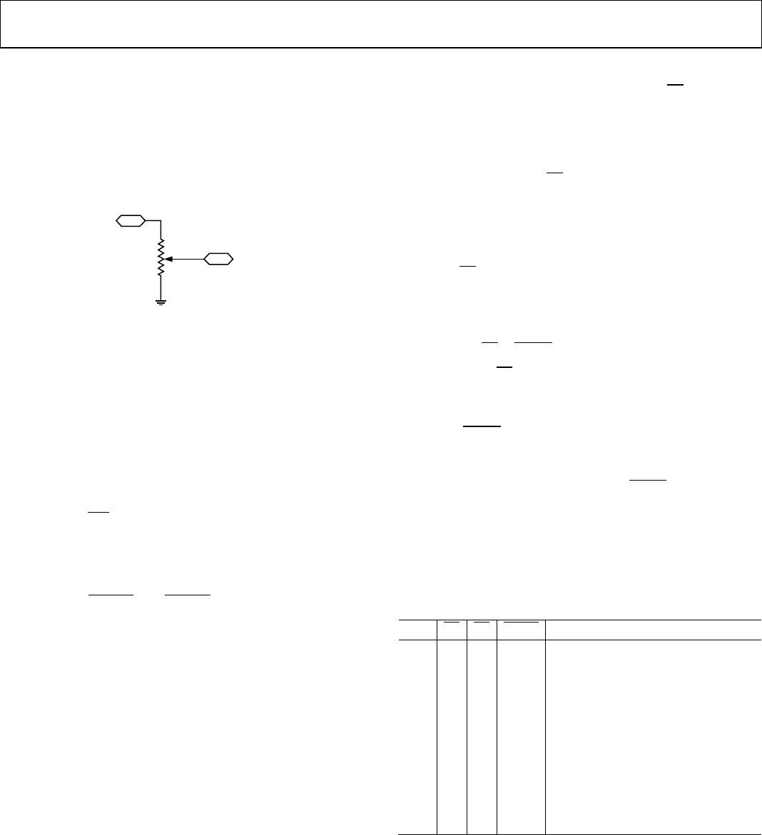
PROGRAMMING THE POTENTIOMETER DIVIDER
Voltage Output Operation
The digital potentiometer easily generates a voltage divider at
Wiper W to Terminal B and Wiper W to Terminal A that is
proportional to the input voltage at Terminal A to Terminal B.
Unlike the polarity of V
DD
to GND, which must be positive,
voltage across Terminal A to Terminal B, Wiper W to Terminal A,
and Wiper W to Terminal B can be at either polarity.
A
V
I
W
B
V
O
01119-026
Figure 26. Potentiometer Mode Configuration
If ignoring the effect of the wiper resistance for the purpose of
approximation, connecting the Terminal A to 30 V and the
Terminal B to ground produces an output voltage at the Wiper W
to Terminal B ranging from 0 V to 1 LSB less than 30 V. Each
LSB of voltage is equal to the voltage applied across Terminals A
and B divided by the 128 positions of the potentiometer divider.
The general equation defining the output voltage at V
W
with
respect to ground for any valid input voltage applied to
Terminals A and B is
A
W
V
D
DV
128
)( =
(3)
A more accurate calculation that includes the effect of wiper
resistance, V
W
, is
B
AB
WA
A
AB
WB
W
V
R
DR
V
R
DR
DV
)(
)(
)( +=
(4)
Operation of the digital potentiometer in the divider mode
results in a more accurate operation over temperature. Unlike
when in rheostat mode, the output voltage in divider mode is
primarily dependent on the ratio, not the absolute values, of the
internal resistors R
WA
and R
WB
. Therefore, the temperature drift
reduces to 5 ppm/°C.
3-WIRE SERIAL BUS DIGITAL INTERFACE
The AD7376 contains a 3-wire digital interface (
CS
, CLK, and
SDI). The 7-bit serial word must be loaded MSB first. The
format of the word is shown in Figure 2. The positive edge-
sensitive CLK input requires clean transitions to avoid clocking
incorrect data into the serial input register. Standard logic
families work well. When
CS
is low, the clock loads data into the
serial register upon each positive clock edge.
The data setup and hold times in Table 3 determine the valid
timing requirements. The AD7376 uses a 7-bit serial input data
register word that is transferred to the internal RDAC register
when the
CS
line returns to logic high. Extra MSB bits are
ignored.
The AD7376 powers up at a random setting. However, the
midscale preset or any desirable preset can be achieved by
manipulating
RS
or
SHDN
with an extra I/O.
When the reset (
RS
) pin is asserted, the wiper resets to the
midscale value. Midscale reset can be achieved dynamically or
during power-up if an extra I/O is used.
When the
SHDN
pin is asserted, the AD7376 opens SW
A
to let
the Terminal A float and to short Wiper W to Terminal B. The
AD7376 consumes negligible power during the shutdown mode
and resumes the previous setting once the
SHDN
pin is released.
On the other hand, the AD7376 can be programmed with any
settings during shutdown. With an extra programmable I/O
asserting shutdown during power-up, this unique feature allows
the AD7376 with programmable preset at any desirable level.
Table 7 shows the logic truth table for all operations.
Table 7. Input Logic Control Truth Table
1
CLK
CS
RS
SHDN
Register Activity
L L H H Enables SR, enables SDO pin.
P L H H Shifts one bit in from the SDI pin. The
seventh previously entered bit is
shifted out of the SDO pin.
X P H H Loads SR data into 7-bit RDAC latch.
X H H H No operation.
X
X
L
H
Sets 7-bit RDAC latch to midscale,
wiper centered, and SDO latch cleared.
X H P H Latches 7-bit RDAC latch to 0x40.
X H H L Opens circuits resistor of Terminal A,
connects Wiper W to Terminal B,
turns off SDO output transistor.
1
P = positive edge, X = don’t care, and SR = shift register.
AD7376
Rev. D | Page 14 of 20
DAISY-CHAIN OPERATION
01119-027
CS
SDI
SERIAL
REGISTER
D
CK
Q
RS
SHDN
SDO
RS
CLK
Figure 27. Detailed SDO Output Schematic of the AD7376
Figure 27 shows the details of the serial data output pin (SDO).
SDO shifts out the SDI content in the previous frame; therefore,
it can be used for daisy-chaining multiple devices. The SDO pin
contains an open-drain N-Channel MOSFET and requires a
pull-up resistor if the SDO function is used.
Users need to tie the SDO pin of one package to the SDI pin of
the next package. For example, in Figure 28, if two AD7376s are
daisy-chained, a total of 14 bits of data are required for each
operation. The first set of seven bits goes to U2; the second set
of seven bits goes to U1.
CS
should be kept low until all 14 bits
are clocked into their respective serial registers. Then
CS
is
pulled high to complete the operation.
When daisy-chaining multiple devices, users may need to
increase the clock period because the pull-up resistor and the
capacitive loading at the SDO to SDI interface may induce a
time delay to subsequent devices.
AD7376
SDOSDI
CLKCS
AD7376
SDO
SDI
CLK
CS
µC
5V
R
PU
2.2kΩ
MOSI
SSSCLK
01119-028
U1 U2
Figure 28. Daisy-Chain Configuration
ESD PROTECTION
All digital inputs are protected with a series input resistor and
an ESD structure shown in Figure 29. These structures apply to
digital input pins
CS
, CLK, SDI,
RS
, and
SHDN
.
INPUT
340Ω
LOGIC
PINS
V
DD
GND
01119-029
Figure 29. Equivalent ESD Protection Circuit
All analog terminals are also protected by ESD protection
diodes, as shown in Figure 30.
V
SS
V
DD
A
W
B
01119-030
Figure 30. Equivalent ESD Protection Analog Pins
TERMINAL VOLTAGE OPERATING RANGE
The AD7376 V
DD
and V
SS
power supplies define the boundary
conditions for proper 3-terminal digital potentiometer oper-
ation. Applied signals present on Terminals A, B, and W that
are more positive than V
DD
or more negative than V
SS
will be
clamped by the internal forward-biased diodes (see Figure 30).
POWER-UP AND POWER-DOWN SEQUENCES
Because of the ESD protection diodes that limit the voltage
compliance at Terminals A, B, and W (see Figure 30), it is
important to power V
DD
/V
SS
before applying voltage to
Terminals A, B, and W. Otherwise, the diodes are forward
biased such that V
DD
/V
SS
are powered unintentionally and affect
the system. Similarly, V
DD
/V
SS
should be powered down last.
The ideal power-up sequence is in the following order: GND,
V
DD
, V
SS
, digital inputs, and V
A
/V
B
/V
W
. The order of powering
V
A
, V
B
, V
W
, and the digital inputs is not important, as long as
they are powered after V
DD
/V
SS
.

AD7376ARUZ100-R7

Mfr. #:
Manufacturer:
Analog Devices Inc.
Description:
Digital Potentiometer ICs IC +/-15V 128-Pos
Lifecycle:
New from this manufacturer.
Delivery:
DHL FedEx Ups TNT EMS
Payment:
T/T Paypal Visa MoneyGram Western Union