AD7376
Rev. D | Page 6 of 20
3-WIRE DIGITAL INTERFACE
Table 4. AD7376 Serial Data-Word Format
1
MSB LSB
D6 D5 D4 D3 D2 D1 D0
2
6
2
0
1
Data is loaded MSB first.
D6 D5 D4 D3 D2 D1 D0
1
SDI
0
1
CLK
0
1
CS
0
1
V
OUT
0
01119-002
RDAC REGISTER LOAD
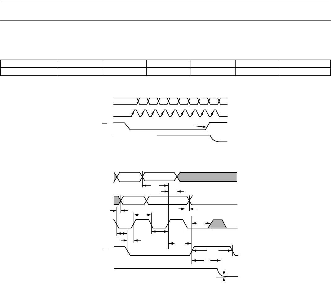
Figure 2. AD7376 3-Wire Digital Interface Timing Diagram
(V
A
= V
DD
, V
B
= 0 V, V
W
= V
OUT
)
±1 LSB ERROR BAND
±1 LSB
t
S
t
CSW
t
CSH
t
CL
V
DD
V
OUT
0V
CS
0
1
t
CSH0
t
CSS
t
CH
0
1
1
0
1
SDI
(DATA IN)
SDO
(DATA OUT)
CLK
D
X
D
X
t
DS
t
DH
D'
X
D'
X
t
PD_MAX
t
CS1
01119-003
0
Figure 3. Detail Timing Diagram
AD7376
Rev. D | Page 7 of 20
ABSOLUTE MAXIMUM RATINGS
T
A
= 25°C, unless otherwise noted.
Table 5.
Parameter Rating
V
DD
to GND −0.3 V to +35 V
V
SS
to GND +0.3 V to −16.5 V
V
DD
to V
SS
−0.3 V to +35 V
V
A
, V
B
, V
W
to GND V
SS
to V
DD
Maximum Current
I
WB
, I
WA
Pulsed ±20 mA
I
WB
Continuous (R
WB
≤ 6 kΩ, A open,
V
DD
/V
SS
= 30 V/0 V)
1
±5 mA
I
WA
Continuous (R
WA
≤ 6 k, B open,
V
DD
/V
SS
= 30 V/0 V)
1
±5 mA
Digital Input and Output Voltages to GND 0 V to V
DD
+ 0.3 V
Operating Temperature Range −40°C to +85°C
Maximum Junction Temperature (T
JMAX
)
2
150°C
Storage Temperature Range −65°C to +150°C
Reflow Soldering
Peak Temperature 260°C
Time at Peak Temperature 20 sec to 40 sec
Package Power Dissipation
(T
JMAX
− T
A
)/θ
JA
Thermal Resistance θ
JA
16-Lead SOIC_W 120°C/W
14-Lead TSSOP 240°C/W
1
Maximum terminal current is bound by the maximum current handling of
the switches, maximum power dissipation of the package, and maximum
applied voltage across any two of the A, B, and W terminals at a given
resistance.
2
Package power dissipation = (T
JMAX
– T
A
)/θ
JA
.
Stresses above those listed under Absolute Maximum Ratings
may cause permanent damage to the device. This is a stress
rating only; functional operation of the device at these or any
other conditions above those indicated in the operational
section of this specification is not implied. Exposure to absolute
maximum rating conditions for extended periods may affect
device reliability.
ESD CAUTION
AD7376
Rev. D | Page 8 of 20
PIN CONFIGURATIONS AND FUNCTION DESCRIPTIONS
01119-004
A
1
B
2
V
SS
3
GND
4
W
14
NC
13
V
DD
12
SDO
11
CS
5
RS
6
CLK
7
SHDN
10
SDI
9
NC
8
NC = NO CONNECT
AD7376
TOP VIEW
(Not to Scale)
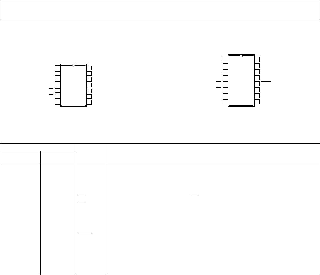
Figure 4. 14-Lead TSSOP Pin Configuration
01119-005
A
1
B
2
V
SS
3
GND
4
W
16
NC
15
V
DD
14
SDO
13
CS
5
SHDN
12
RS
6
SDI
11
CLK
7
NC
10
NC
8
NC
9
NC = NO CONNECT
AD7376
TOP VIEW
(Not to Scale)
Figure 5. 16-Lead SOIC_W Pin Configuration
Table 6.Pin Function Descriptions
Pin No.
14-Lead
TSSOP
16-Lead
SOL Mnemonic Description
1 1 A A Terminal. V
SS
≤ V
A
≤ V
DD
.
2 2 B B Terminal. V
SS
≤ V
B
≤ V
DD
.
3 3 V
SS
Negative Power Supply.
4 4 GND Digital Ground.
5 5
CS
Chip Select Input, Active Low. When
CS
returns high, data is loaded into the wiper register.
6 6
RS
Reset to Midscale.
7 7 CLK Serial Clock Input. Positive edge triggered.
8 8, 9, 10 NC No Connect. Let it float or ground.
9 11 SDI Serial Data Input (data loads MSB first).
10 12
SHDN
Shutdown. A terminal open ended; W and B terminals shorted. Can be used as
programmable preset.
1
11
13
SDO
Serial Data Output.
12 14 V
DD
Positive Power Supply.
13 15 NC No Connect. Let it float or ground.
14 16 W Wiper Terminal. V
SS
≤ V
W
≤ V
DD
.
1
Assert shutdown and program the device during power-up. Then, deassert the shutdown to achieve the desirable preset level.

AD7376ARUZ100-R7

Mfr. #:
Manufacturer:
Analog Devices Inc.
Description:
Digital Potentiometer ICs IC +/-15V 128-Pos
Lifecycle:
New from this manufacturer.
Delivery:
DHL FedEx Ups TNT EMS
Payment:
T/T Paypal Visa MoneyGram Western Union