AD7376
Rev. D | Page 17 of 20
AUDIO VOLUME CONTROL
Because of its good THD performance and high voltage
capability, the AD7376 can be used for digital volume control. If
AD7376 is used directly as an audio attenuator or gain amplifier,
a large step change in the volume level at any arbitrary time can
lead to an abrupt discontinuity of the audio signal, causing an
audible zipper noise. To prevent this, a zero-crossing window
detector can be inserted to the
CS
line to delay the device
update until the audio signal crosses the window. Since the
input signal can operate on top of any dc levels rather than
absolute zero volt level, zero-crossing, in this case, means the
signal is ac-coupled and the dc offset level is the signal zero
reference point.
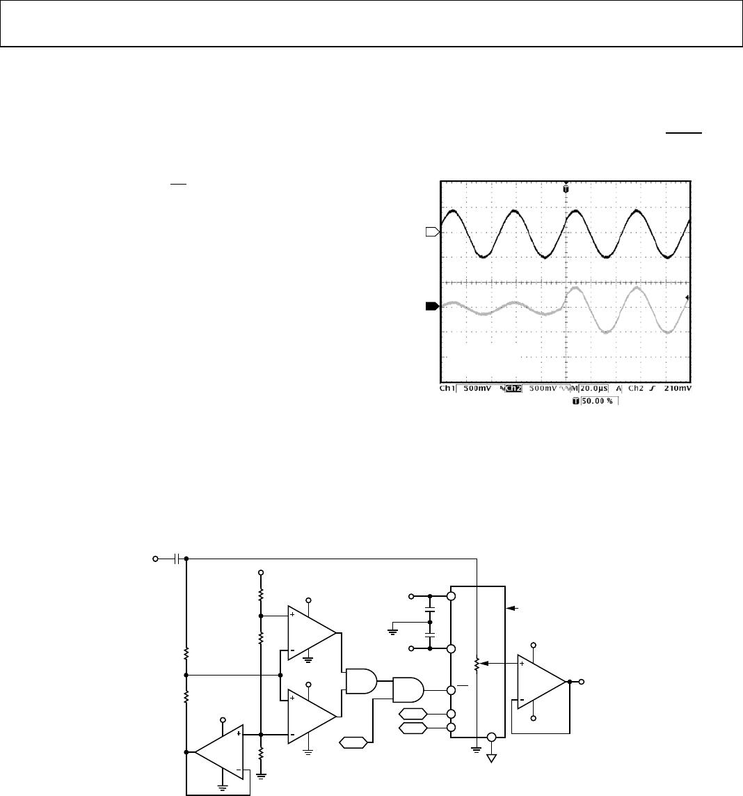
The configuration to reduce zipper noise and the result of using
this configuration are shown in Figure 35 and Figure 34,
respectively. The input is ac-coupled by C1 and attenuated
down before feeding into the window comparator formed by
U2, U3, and U4B. U6 is used to establish the signal zero
reference. The upper limit of the comparator is set above its
offset and, therefore, the output pulses high whenever the input
falls between 2.502 V and 2.497 V (or 0.005 V window) in this
example. This output is AND’ed with the chip select signal such
that the AD7376 updates whenever the signal crosses the
window. To avoid constant update of the device, the chip select
signal should be programmed as two pulses, rather than the one
shown in Figure 2.
In Figure 34, the lower trace shows that the volume level
changes from a quarter scale to full scale when a signal change
occurs near the zero-crossing window.
The AD7376 shutdown sleep-mode programming feature can
be used to mute the device at power-up by holding
SHDN
low
and programming zero scale.
01119-035
CHANNEL 1
FREQ = 20.25kHz
1.03V p-p
1
2
NOTES
1. THE LOWER TRACE SHOWS THAT THE VOLUME LEVEL
CHANGES FROM QUARTER SCALE TO FULL SCALE, WITH THE
CHANGE OCCURRING NEAR THE ZERO-CROSSING WINDOW.
Figure 34. Input (Trace 1) and Output (Trace 2) of the Circuit in Figure 35
V
DD
V
SS
CS
CLK
SDI
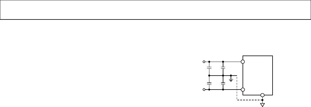
V+
V–
AD7376
100kΩ
+15V
–15V
C3
0.1µF
C2
0.1µF
A
B
W
GND
SDI
CLK
U1
+15V
–15V
V
OUT
U5
01119-034
CS
V+
V+
V–
V–
ADCM371
ADCM371
+5V
+5V
U3
U2
R1
100kΩ
R2
200Ω
+5V
V
IN
U4A
U4B
16
2
4
5
7408
7408
V+
V–
AD8541
+5V
U6
R3
100Ω
R4
90kΩ
R5
10kΩ
C1
1µF
Figure 35. Audio Volume Control with Zipper Noise Reduction