10
IDT72V801/72V8211/72V821/72V831/72V841/72V851 3.3V DUAL CMOS SyncFIFO
TM
DUAL 256 x 9, DUAL 512 x 9, DUAL 1K x 9, DUAL 2K x 9, DUAL 4K x 9, DUAL 8K x 9
COMMERCIAL AND INDUSTRIAL
TEMPERATURE RANGES
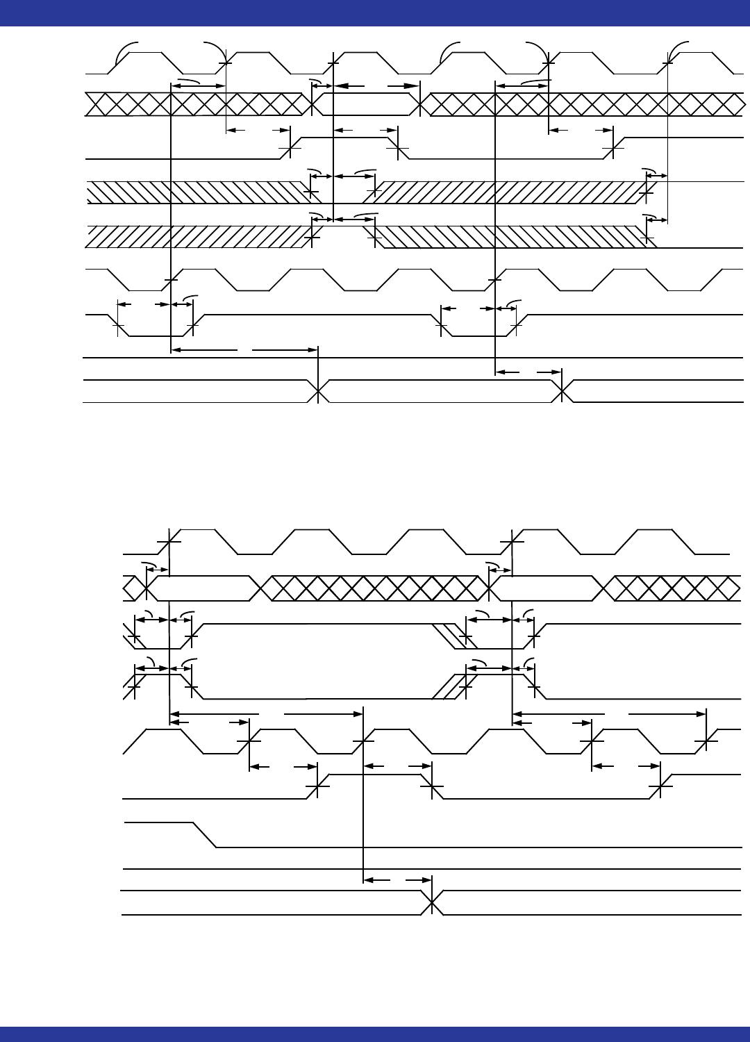
Figure 6. Read Cycle Timing
NOTE:
1. When tSKEW1 minimum specification, tFRL = tCLK + tSKEW1
When tSKEW1 < minimum specification, tFRL = 2tCLK + tSKEW1 or tCLK + tSKEW1
The Latency Timings apply only at the Empty Boundary (EFA, EFB = LOW).
Figure 7. First Data Word Latency Timing
NOTE:
1. tSKEW1 is the minimum time between a rising WCLKA (WCLKB) edge and a rising RCLKA (RCLKB) edge for EFA (EFB) to change during the current clock cycle. If the time
between the rising edge of RCLKA (RCLKB) and the rising edge of WCLKA (WCLKB) is less than tSKEW1, then EFA (EFB) may not change state until the next RCLKA (RCLKB)
edge.
t
ENH
t
ENS
NO OPERATION
t
OLZ
VALID DATA
t
SKEW1
(1)
t
CLK
t
CLKH
t
CLKL
t
REF
t
REF
t
A
t
OE
t
OHZ
RCLKA (RCLKB)
RENA1, RENA2
(RENB1, RENB2)
EFA (EFB)
QA
0
- QA
8
(QB
0
- QB
8
)
OEA (OEB)
WCLKA, WCLKB
WENA1 (WENB1)
WENA2 (WENB2)
4093 drw 08
tDS
D0 (First Valid
t
SKEW1
D0 D1
D3D2D1
tENS
tFRL
(1)
tREF
tA
tOLZ
tOE
tA
WCLKA
(WCLKB)
DA
0 - DA8
(DB0 - DB8)
WENA2 (WENB2)
(If Applicable)
RCLKA
(RCLKB)
EFA (EFB)
RENA1, RENA2
(RENB1, RENB2)
QA
0 - QA8
(QB0 - QB8)
OEA (OEB)
WENA1
(WENB1)
4093 drw 09
tENS
tENS
11
IDT72V801/72V8211/72V821/72V831/72V841/72V851 3.3V DUAL CMOS SyncFIFO
TM
DUAL 256 x 9, DUAL 512 x 9, DUAL 1K x 9, DUAL 2K x 9, DUAL 4K x 9, DUAL 8K x 9
COMMERCIAL AND INDUSTRIAL
TEMPERATURE RANGES
NOTE:
1. Only one of the two Write Enable inputs, WEN1 or WEN2, needs to go inactive to inhibit writes to the FIFO.
Figure 8. Full Flag Timing
Figure 9. Empty Flag Timing
NOTE:
1. When tSKEW1 minimum specification, tFRL maximum = tCLK + tSKEW1
When tSKEW1 < minimum specification, tFRL maximum = 2tCLK + tSKEW1 or tCLK + tSKEW1
The Latency Timings apply only at the Empty Boundary (EFA, EFB = LOW).
WCLKA
(WCLKB)
DA
0
- DA
8
(DB
0
- DB
8
)
FFA (FFB)
WENA1
(WENB1)
WENA2
(WENB2)
(If Applicable)
RCLKA
(RCLKB)
RENA1
(RENB2)
QA
0
- QA
8
(QB
0
- QB
8
)
OEA
(OEB)
4093 drw 10
t
SKEW1
t
DS
t
SKEW1
t
ENH
t
ENH
NEXT DATA READDATA READ
t
WFF
t
WFF
t
WFF
t
ENS
t
ENS
DATA IN OUTPUT REGISTER
LOW
NO WRITE
NO WRITE
t
A
t
A
t
ENS
t
ENS
t
ENS
(1)
t
ENS
(1)
t
ENH
t
ENH
NO WRITE
t
DH
t
A
t
DS
t
DS
t
ENS
t
ENH
t
ENS
t
ENH
t
ENS
t
ENH
t
ENS
t
ENH
DATA WRITE 2
WCLKA (WCLKB)
DA
0
- DA
8
(DB
0
- DB
8
)
RCLKA (RLCKB)
EFA (EFB)
RENA1, RENA2
(RENB1, RENB2)
OEA (OEB)
QA
0
- QA
8
(QB
0
- QB
8
)
DATA READ
t
SKEW1
(1)
t
FRL
t
FRL
DATA IN OUTPUT REGISTER
(1)
t
SKEW1
LOW
WENA2 (WENB2)
(If Applicable)
t
REF
t
REF
t
REF
WENA1, (WENB1)
4093 drw 11
DATA WRITE 1
12
IDT72V801/72V8211/72V821/72V831/72V841/72V851 3.3V DUAL CMOS SyncFIFO
TM
DUAL 256 x 9, DUAL 512 x 9, DUAL 1K x 9, DUAL 2K x 9, DUAL 4K x 9, DUAL 8K x 9
COMMERCIAL AND INDUSTRIAL
TEMPERATURE RANGES
NOTES:
1. m = PAF offset.
2. (256-m) words for the IDT72V801, (512-m) words the IDT72V811, (1,024-m) words for the IDT72V821, (2,048-m) words for the IDT72V831, (4,096-m) words for the IDT72V841,
or (8,192-m) words for the IDT72V851.
3. tSKEW2 is the minimum time between a rising RCLKA (RCLKB) edge and a rising WCLKA (WCLKB) edge for PAFA (PAFB) to change during that clock cycle. If the time between
the rising edge of RCLKA (RCLKB) and the rising edge of WCLKA (WCLKB) is less than tSKEW2, then PAFA (PAFB) may not change state until the next WCLKA (WCLKB)
rising edge.
4. If a write is performed on this rising edge of the Write Clock, there will be Full - (m-1) words in FIFO A (B) when PAFA (PAFB) goes LOW.
Figure 10. Programmable Full Flag Timing
Figure 11. Programmable Empty Flag Timing
NOTES:
1. n = PAE offset.
2. tSKEW2 is the minimum time between a rising WCLKA (WCLKB) edge and a rising RCLKA (RCLKB) edge for PAEA (PAEB) to change during that clock cycle. If the time between
the rising edge of WCLKA (WCLKB) and the rising edge of RCLKA (RCLKB) is less than tSKEW2, then PAEA (PAEB) may not change state until the next RCLKA (RCLKB)
rising edge.
3. If a read is performed on this rising edge of the Read Clock, there will be Empty + (n-1) words in FIFO A (B) when PAEA (PAEB) goes LOW.
t
ENS
t
ENH
t
ENS
t
ENH
t
ENS
t
ENH
WCLKA
(WCLKB)
WENA1
(WENB1
WENA2
(WENB2)
(If Applicable)
PAFA
(PAFB)
RCLKA
(RCLKB)
RENA1, RENA2
(RENB1, RENB2)
(4)
t
PAF
(1)
Full - (m+1) words in FIFO
Full - m words in FIFO
(2)
t
CLKH
t
CLKL
t
SKEW2
(3)
t
PAF
4093 drw 12
WCLKA
(WCLKB)
WENA1
(WENB1)
WENA2
(WENB2)
(If Applicable)
PAEA,
PAEB
RCLKA
(RCLKB)
RENA1, RENA2
(RENB1, RENB2)
t
ENS
t
ENH
t
ENS
t
ENH
t
SKEW2
(2)
t
ENS
t
ENH
t
PAE
t
PAE
(3)
(1)
n words in FIFO
n+1 words in FIFO
t
CLKH
t
CLKL
4093 drw 13

72V841L15PFI

Mfr. #:
Manufacturer:
IDT
Description:
FIFO 3.3 V DUAL 4K X 9
Lifecycle:
New from this manufacturer.
Delivery:
DHL FedEx Ups TNT EMS
Payment:
T/T Paypal Visa MoneyGram Western Union