8
IDT72V801/72V8211/72V821/72V831/72V841/72V851 3.3V DUAL CMOS SyncFIFO
TM
DUAL 256 x 9, DUAL 512 x 9, DUAL 1K x 9, DUAL 2K x 9, DUAL 4K x 9, DUAL 8K x 9
COMMERCIAL AND INDUSTRIAL
TEMPERATURE RANGES
OUTPUTSOUTPUTS
OUTPUTSOUTPUTS
OUTPUTS
::
::
:
Full Flag (FFA, FFB) — FFA (FFB) will go LOW, inhibiting further write
operations, when Array A (B) is full. If no reads are performed after reset,
FFA (FFB) will go LOW after 256 writes to the IDT72V801's FIFO A (B), 512
writes to the IDT72V811's FIFO A (B), 1,024 writes to the IDT72V821's FIFO
A (B), 2,048 writes to the IDT72V831's FIFO A (B), 4,096 writes to the
IDT72V841's FIFO A (B), or 8,192 writes to the IDT72V851's FIFO A (B).
FFA ( FFB) is synchronized with respect to the LOW-to-HIGH transition of
the Write Clock WCLKA (WCLKB).
Empty Flag (EFA, EFB) — EFA ( EFB) will go LOW, inhibiting further read
operations, when the read pointer is equal to the write pointer, indicating that
Array A (B) is empty.
EFA ( EFB) is synchronized with respect to the LOW-to-HIGH transition of
the Read Clock RCLKA (RCLKB).
Programmable Almost–Full Flag (PAFA, PAFB) —
PAFA ( PAFB) will go
LOW when the amount of data in Array A (B) reaches the Almost-Full condition.
If no reads are performed after reset, PAFA ( PAFB) will go LOW after (256-m)
writes to the IDT72V801's FIFO A (B), (512-m) writes to the IDT72V811's FIFO
A (B), (1,024-m) writes to the IDT72V821's FIFO A (B), (2,048-m) writes to
the IDT72V831's FIFO A (B), (4,096-m) writes to the IDT72V841's FIFO A
(B), or (8,1912-m) writes to the IDT72V851's FIFO A (B).
FFA ( FFB) is synchronized with respect to the LOW-to-HIGH transition of
the Write Clock WCLKA (WCLKB). The offset “m” is defined in the Full Offset
Registers.
If there is no Full offset specified, PAFA ( PAFB) will go LOW at Full-7 words.
PAFA ( PAFB) is synchronized with respect to the LOW-to-HIGH transition
of the Write Clock WCLKA (WCLKB).
Programmable Almost–Empty Flag (PAEA, PAEB) — PAEA ( PAEB) will
go LOW when the read pointer is "n+1" locations less than the write pointer.
The offset "n" is defined in the Empty Offset Registers. If no reads are performed
after reset, PAEA (PAEB) will go HIGH after "n+1" writes to FIFO A (B).
If there is no Empty offset specified, PAEA ( PAEB) will go LOW at Empty+7
words.
PAEA ( PAEB) is synchronized with respect to the LOW-to-HIGH transition
of the Read Clock RCLKA (RCLKB).
Data Outputs (QA0 – QA8, QB0 – QB8 ) — QA0 - QA8 are the nine data
outputs for memory array A, QB0 - QB8 are the nine data outputs for memory
array B.
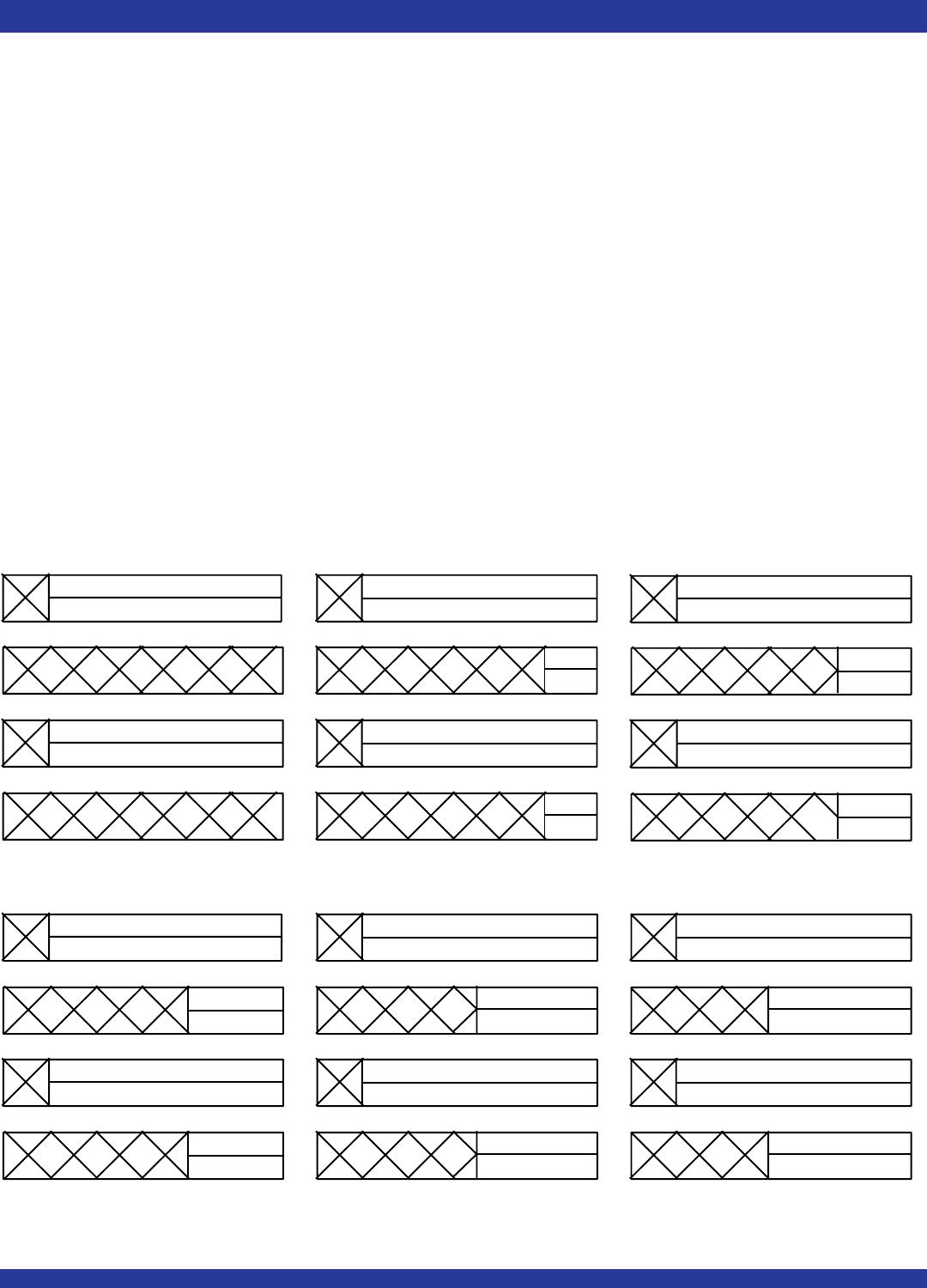
NUMBER OF WORDS IN ARRAY A FFA PAFA PAEA E FA
NUMBER OF WORDS IN ARRAY B FFB PAFB PAEB E FB
IDT72V801 IDT72V811 IDT72V821
000HHLL
1 to n
(1)
1 to n
(1)
1 to n
(1)
HH LH
(n+1) to (256-(m+1)) (n+1) to (512-(m+1)) (n+1) to (1,024-(m+1))
HHHH
(256-m)
(2)
to 255 (512-m)
(2)
to 511 (1,024-m)
(2)
to 1,023 H L H H
256 512 1,024 L L H H
NOTES:
1. n = Empty Offset (n = 7 default value)
2. m = Full Offset (m = 7 default value)
NUMBER OF WORDS IN ARRAY A FFA PAFA PAEA E FA
NUMBER OF WORDS IN ARRAY B FFB PAFB PAEB E FB
IDT72V831 IDT72V841 IDT72V851
000HHLL
1 to n
(1)
1 to n
(1)
1 to n
(1)
HH LH
(n+1) to (2,048-(m+1)) (n+1) to (4,096-(m+1)) (n+1) to (8,192-(m+1))
HHHH
(2,048-m)
(2)
to 2,047 (4,096-m)
(2)
to 4,095 (8,192-m)
(2)
to 8,191 H L H H
2,048 4,096 8,192 L L H H
TABLE 1: STATUS FLAGS FOR A AND B FIFOS