13
IDT72V801/72V8211/72V821/72V831/72V841/72V851 3.3V DUAL CMOS SyncFIFO
TM
DUAL 256 x 9, DUAL 512 x 9, DUAL 1K x 9, DUAL 2K x 9, DUAL 4K x 9, DUAL 8K x 9
COMMERCIAL AND INDUSTRIAL
TEMPERATURE RANGES
Figure 12. Write Offset Register Timing
Figure 13. Read Offset Register Timing
WCLKA (WCLKB)
LDA (LDB)
WENA1 (WENB1)
DA
0
- DA
7
(DB
0
- DB
7
)
4093 drw 14
t
ENS
t
ENH
t
ENS
t
DS
t
DH
PAF OFFSET
(MSB)
PAF OFFSET
(LSB)
PAE OFFSET
(MSB)
PAE OFFSET
(LSB)
t
CLK
t
CLKL
t
CLKH
RCLKA (RCLKB)
LDA (LDB)
RENA1, RENA2
(RENB1, RENB2)
QA
0 - QA7
(QB0 - QB7)
4093 drw 15
tENS
tENH
tENS
DATA IN OUTPUT REGISTER
EMPTY OFFSET
(LSB)
EMPTY OFFSET
(MSB)
FULL OFFSET
(LSB)
FULL OFFSET
(MSB)
tCLK
tA
tCLKLtCLKH
14
IDT72V801/72V8211/72V821/72V831/72V841/72V851 3.3V DUAL CMOS SyncFIFO
TM
DUAL 256 x 9, DUAL 512 x 9, DUAL 1K x 9, DUAL 2K x 9, DUAL 4K x 9, DUAL 8K x 9
COMMERCIAL AND INDUSTRIAL
TEMPERATURE RANGES
OPERATING CONFIGURATIONS
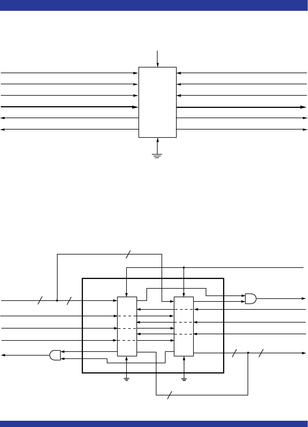
SINGLE DEVICE CONFIGURATION — When FIFO A (B) is in a Single
Device Configuration, the Read Enable 2 RENA2 ( RENB2) control input can
Figure 15. Block diagram of the two FIFOs contained in one IDT72V801/72V811/72V821/72V831/72V841/72V851
configured for an 18-bit width-expansion
be grounded (see Figure 14). In this configuration, the Write Enable 2/Load
WENA2/LDA (WENB2/LDB) pin is set LOW at Reset so that the pin operates
as a control to load and read the programmable flag offsets.
Figure 14. Block Diagram of One of the IDT72V801/72V811/72V821/72V831/72V841/72V851's
two FIFOs configured as a single device
WIDTH EXPANSION CONFIGURATION — Word width may be in-
creased simply by connecting the corresponding input control signals of
FIFOs A and B. A composite flag should be created for each of the end-
point status flags EFA and EFB, also FFA and FFB). The partial status flags PAEA,
PAFB, PAEA and PAFB can be detected from any one device. Figure 15
demonstrates an 18-bit word width using the two FIFOs contained in one
IDT72V801/72V811/72V821/72V831/72V841/72V851. Any word width can
be attained by adding additional IDT72V801/72V811/72V821/72V831/
72V841/72V851s.
When these devices are in a Width Expansion Configuration, the Read
Enable 2 (RENA2 and RENB2) control inputs can be grounded (see Figure
15). In this configuration, the Write Enable 2/Load (WENA2/LDA, WENB2/LDB)
pins are set LOW at Reset so that the pin operates as a control to load and read
the programmable flag offsets.
QA
0
- QA
8
(QB
0
- QB
8
)
DA
0
- DA
8
(DB
0
- DB
8
)
RSA (RSB)
RCLKA (RCLKB)
RENA1 (RENB1)
OEA (OEB)
EFA (EFB)
PAEA (PAEB)
RENA2 (RENB2)
WCLKA (WCLKB)
WENA1 (WENB1)
WENA2/LDA (WENB2/LDB)
FFA (FFB)
PAFA (PAFB)
IDT
72V801
72V811
72V821
72V831
72V841
72V851
FIFO
A (B)
4093 drw 16
DATA IN
WRITE CLOCK
18
9
RSB
READ CLOCK
9
18
RENB2RENA2
WRITE ENABLE
FFA
EFB
OUTPUT ENABLE
READ ENABLE
9
WRITE ENABLE/LOAD
FFB
EFA
RSA
RAM
ARRAY
A
DATA OUT
RCLKA
EMPTY FLAG
RENB1
RENA1
OEB
OEA1
RCLKB
WCLKA
WCLKB
WENA1
WENB1
DA0 - DA8
DB0 - DB8
QA0 - QA8
QB0 - QB8
WENA2/LDA
2WENB2/LDB
RESET
9
FULL FLAG
4093 drw 17
RAM
ARRAY
B
256x9
512x9
1,024x9
2,048x9
4,096x9
8,192x9
256x9
512x9
1,024x9
2,048x9
4,096x9
8,192x9
15
IDT72V801/72V8211/72V821/72V831/72V841/72V851 3.3V DUAL CMOS SyncFIFO
TM
DUAL 256 x 9, DUAL 512 x 9, DUAL 1K x 9, DUAL 2K x 9, DUAL 4K x 9, DUAL 8K x 9
COMMERCIAL AND INDUSTRIAL
TEMPERATURE RANGES
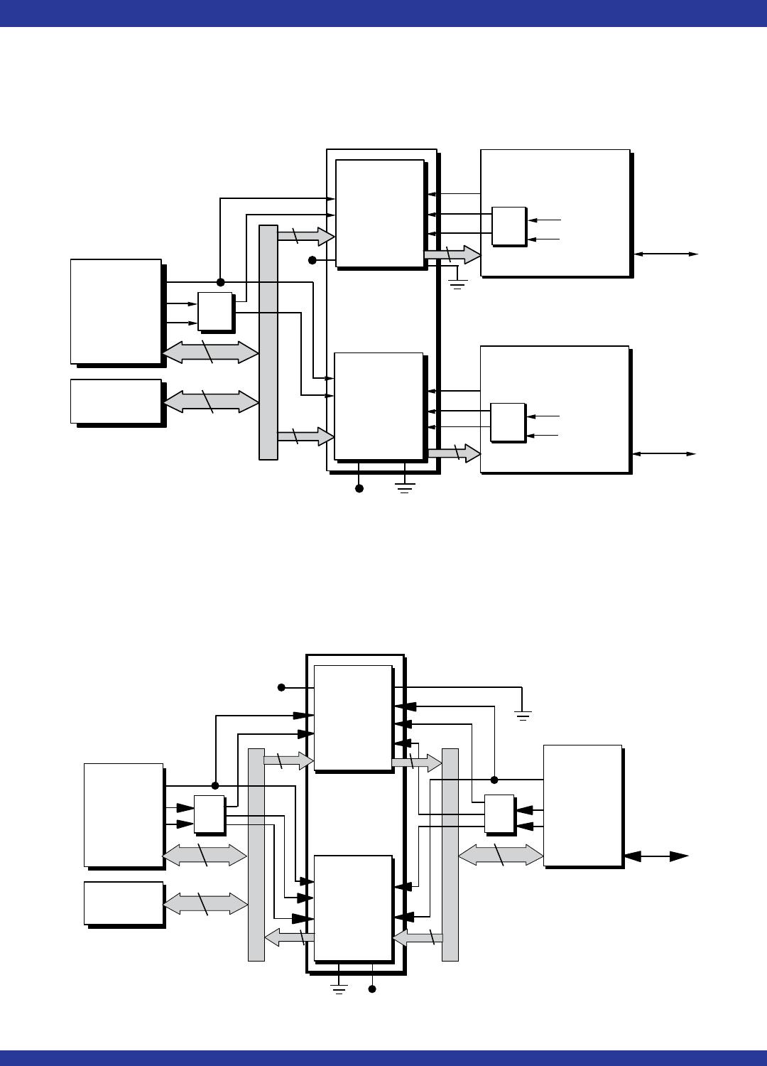
the intermixed data according to type, sending one kind to FIFO A and the other
kind to FIFO B. Then, at the outputs, each data type is transferred to its
appropriate destination. Additional IDT72V801/72V811/72V821/72V831/
72V841/72V851s permit more than two priority levels. Priority buffering is
particularly useful in network applications.
TWO PRIORITY DATA BUFFER
CONFIGURATION
The two FIFOs contained in the IDT72V801/72V811/72V821/72V831/
72V841/72V851 can be used to prioritize two different types of data shared
on a system bus. When writing from the bus to the FIFO, control logic sorts
Figure 16. Block Diagram of Two Priority Configuration
Figure 17. Block Diagram of Bidirectional Configuration
BIDIRECTIONAL CONFIGURATION
The two FIFOs of the IDT72V801/72V811/72V821/72V831/72V841/
72V851 can be used to buffer data flow in two directions. In the example that
follows, a processor can write data to a peripheral controller via FIFO A, and,
in turn, the peripheral controller can write the processor via FIFO B.
RAM ARRAY A
Processor
Data
D
A0
-D
A8
Q
A0
-Q
A8
OEA
RENA
Address
IDT
72V801
72V811
72V821
72V831
72V841
72V851
D
B0
-D
B8
Q
B0
-Q
B8
OEB2WENB1
Control
Logic
RAM
9-bit bus
RCLKA
WCLKB
Control
9
9
9
9
WCLKA
WENA1
RAM ARRAY B
RENB1
Clock
RCLKB
WENB2
RENB2
WENA2
RENA2
V
CC
V
CC
9
9
Voice
Processing
Card
Data
I/O Data
Clock
Control
Logic
Address
Control
Image
Processing
Card
Data
I/O Data
Clock
Control
Logic
Address
Control
4093 drw 18
RAM ARRAY A
Processor
Peripheral
Controller
Data
DA0-DA8
QA0-QA8
Data
OEA
RENA1
Address
I/O Data
IDT
72V801
72V811
72V821
72V831
72V841
72V851
DB0-DB8
QB0-QB8
OEB
WENB1
Control
Logic
RAM
9-bit bus
9-bit bus
RCLKA
WCLKB
Control
9
9
9
9
9
9
WCLKA
WENA1
RAM ARRAY B
RENB1
Clock
RCLKB
DMA Clock
Control
Logic
Address
Control
9
WENB2
RENB2
WENA2
RENA2
V
CC
V
CC
4093 drw 19

72V841L15PFI

Mfr. #:
Manufacturer:
IDT
Description:
FIFO 3.3 V DUAL 4K X 9
Lifecycle:
New from this manufacturer.
Delivery:
DHL FedEx Ups TNT EMS
Payment:
T/T Paypal Visa MoneyGram Western Union