6
IDT72V801/72V8211/72V821/72V831/72V841/72V851 3.3V DUAL CMOS SyncFIFO
TM
DUAL 256 x 9, DUAL 512 x 9, DUAL 1K x 9, DUAL 2K x 9, DUAL 4K x 9, DUAL 8K x 9
COMMERCIAL AND INDUSTRIAL
TEMPERATURE RANGES
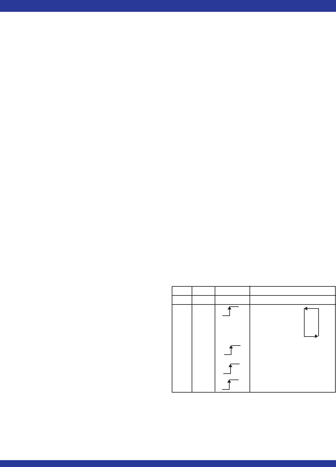
LDA WENA1 WCLKA OPERATION ON FIFO A
LDB WENB1 WCLKB OPERATION ON FIFO B
0 0 Empty Offset (LSB)
Empty Offset (MSB)
Full Offset (LSB)
Full Offset (MSB)
0 1 No Operation
1 0 Write Into FIFO
1 1 No Operation
Figure 2. Writing to Offset Registers for FIFOs A and B
When either of the two Read Enable, RENA1, RENA2 (RENB1, RENB2)
associated with FIFO A (B) is HIGH, the output register holds the previous data
and no new data is allowed to be loaded into the register.
When all the data has been read from FIFO A (B), the Empty Flag, EFA
(EFB) will go LOW, inhibiting further read operations. Once a valid write
operation has been accomplished, EFA (EFB) will go HIGH after tREF and a
valid read can begin. The Read Enables, RENA1, RENA2 (RENB1, RENB2)
are ignored when FIFO A (B) is empty.
Output Enable (OEA, OEB) — When Output Enable, OEA (OEB) is
enabled (LOW), the parallel output buffers of FIFO A (B) receive data from their
respective output register. When Output Enable, OEA (OEB) is disabled
(HIGH), the QA (QB) output data bus is in a high-impedance state.
Write Enable 2/Load (WENA2/LDA, WENB2/LDB) — This is a dual-
purpose pin. FIFO A (B) is configured at Reset to have programmable flags
or to have two write enables, which allows depth expansion. If WENA2/LDA
(WENB2/LDB) is set HIGH at Reset, RSA = LOW (RSB = LOW), this pin operates
as a second Write Enable pin.
If FIFO A (B) is configured to have two write enables, when Write Enable
1, WENA1 ( WENB1) is LOW and WENA2/LDA (WENB2/LDB) is HIGH, data can
be loaded into the input register and RAM array on the LOW-to-HIGH transition
of every Write Clock, WCLKA (WCLKB). Data is stored in the array sequentially
and independently of any on-going read operation.
In this configuration, when WENA1 ( WENB1) is HIGH and/or WENA2/LDA
(WENB2/LDB) is LOW, the input register of Array A holds the previous data
and no new data is allowed to be loaded into the register.
To prevent data overflow, the Full Flag, FFA ( FFB) will go LOW, inhibiting
further write operations. Upon the completion of a valid read cycle, FFA ( FFB)
will go HIGH after tWFF, allowing a valid write to begin. WENA1, (WENB1) and
WENA2/LDA (WENB2/LDB) are ignored when the FIFO is full.
FIFO A (B) is configured to have programmable flags when the WENA2/
LDA (WENB2/LDB) is set LOW at Reset, RSA = LOW (RSB = LOW). Each FIFO
SIGNAL DESCRIPTIONS
FIFO A and FIFO B are identical in every respect. The following description
explains the interaction of input and output signals for FIFO A. The correspond-
ing signal names for FIFO B are provided in parentheses.
INPUTS:
Data In (DA0 – DA8, DB0 – DB8) — DA0 - DA8 are the nine data inputs
for memory array A. DB0 - DB8 are the nine data inputs for memory array B.
CONTROLS:
Reset (RSA, RSB) — Reset of FIFO A (B) is accomplished whenever RSA
(RSB) input is taken to a LOW state. During reset, the internal read and write
pointers associated with the FIFO are set to the first location. A reset is required
after power-up before a write operation can take place. The Full Flag, FFA
(FFB) and Programmable Almost-Full Flag, PAFA ( PAFB) will be reset to HIGH
after tRSF. The Empty Flag, EFA ( EFB) and Programmable Almost-Empty Flag,
PAEA ( PAEB) will be reset to LOW after tRSF. During reset, the output register
is initialized to all zeros and the offset registers are initialized to their default
values.
Write Clock (WCLKA, WCLKB) — A write cycle to Array A (B) is initiated
on the LOW-to-HIGH transition of WCLKA (WCLKB). Data set-up and hold
times must be met with respect to the LOW-to-HIGH transition of WCLKA
(WCLKB). The Full Flag, FFA (FFB) and Programmable Almost-Full Flag,
PAFA ( PAFB) are synchronized with respect to the LOW-to-HIGH transition of
the Write Clock, WCLKA (WCLKB).
The Write and Read clock can be asynchronous or coincident.
Write Enable 1 (WENA1, WENB1) — If FIFO A (B) is configured for
programmable flags, WENA1 ( WENB1) is the only enable control pin. In this
configuration, when WENA1 ( WENB1) is LOW, data can be loaded into the input
register of RAM Array A (B) on the LOW-to-HIGH transition of every Write
Clock, WCLKA (WCLKB). Data is stored in Array A (B) sequentially and
independently of any on-going read operation.
In this configuration, when WENA1 (WENB1) is HIGH, the input register
holds the previous data and no new data is allowed to be loaded into the
register.
If the FIFO is configured to have two write enables, which allows for depth
expansion. See Write Enable 2 paragraph below for operation in this
configuration.
To prevent data overflow, FFA ( FFB) will go LOW, inhibiting further write
operations. Upon the completion of a valid read cycle, the FFA ( FFB) will go
HIGH after tWFF, allowing a valid write to begin. WENA1 ( WENB1) is ignored
when FIFO A (B) is full.
Read Clock (RCLKA, RCLKB) — Data can be read from Array A (B)
on the LOW-to-HIGH transition of RCLKA (RCLKB). The Empty Flag, EFA
(EFB) and Programmable Almost-Empty Flag, PAEA ( PAEB) are synchronized
with respect to the LOW-to-HIGH transition of RCLKA (RCLKB).
The Write and Read Clock can be asynchronous or coincident.
Read Enables (RENA1, RENA2, RENB1, RENB2) — When both Read
Enables, RENA1, RENA2 ( RENB1, RENB2) are LOW, data is read from Array
A (B) to the output register on the LOW-to-HIGH transition of the Read Clock,
RCLKA (RCLKB).
NOTE: 4093 tbl 08
1. For the purposes of this table, WENA2 and WENB2 = VIH.
2. The same selection sequence applies to reading from the registers. RENA1 and RENA2
(RENB1 and RENB2) are enabled and read is performed on the LOW-to-HIGH transition
of RCLKA (RCLKB).

