2.7 V to 5.5 V, Serial-Input,
Voltage-Output, 12-/16-Bit DAC
Data Sheet
AD5512A/AD5542A
Rev. C Document Feedback
Information furnished by Analog Devices is believed to be accurate and reliable. However, no
responsibility is assumed by Analog Devices for its use, nor for any infringements of patents or other
rights of third parties that may result from its use. Specifications subject to change without notice. No
license is granted by implication or otherwise under any patent or patent rights of Analog Devices.
Trademarks and registered trademarks are the property of their respective owners.
One Technology Way, P.O. Box 9106, Norwood, MA 02062-9106, U.S.A.
Tel: 781.329.4700 ©2010–2017 Analog Devices, Inc. All rights reserved.
Technical Support www.analog.com
FEATURES
12-/16-bit resolution
1 LSB INL
11.8 nV/√Hz noise spectral density
1 µs settling time
1.1 nV-sec glitch energy
0.05 ppm/°C temperature drift
5 kV HBM ESD classification
0.375 mW power consumption at 3 V
2.7 V to 5.5 V single-supply operation
Hardware
CLR
and
LDAC
functions
50 MHz SPI-/QSPI-/MICROWIRE-/DSP-compatible interface
Power-on reset clears DAC output to midscale
Available in 3 mm × 3 mm, 10-/16-lead LFCSP and
16-lead TSSOP
APPLICATIONS
Automatic test equipment
Precision source-measure instruments
Data acquisition systems
Medical and aerospace instrumentation
Communication equipment
GENERAL DESCRIPTION
The AD5512A/AD5542A are single, 12-/16-bit, serial input,
unbuffered voltage output digital-to-analog converters (DAC)
that operate from a single 2.7 V to 5.5 V supply. The DAC
output range extends from 0 V to V
REF
and is guaranteed
monotonic, providing 1 LSB INL accuracy at 16 bits without
adjustment over the full specified temperature range of −40°C
to +85°C (AD5542A) or −40°C to +125°C (AD5512A).
Offering unbuffered outputs, the AD5512A/AD5542A achieve
a 1 μs settling time with low offset errors ideal for high speed
open loop control.
The AD5512A/AD5542A incorporate a bipolar mode of
operation that generates a ±V
REF
output swing. The
AD5512A/AD5542A also include Kelvin sense connections for
the reference and analog ground pins to reduce layout sensitivity.
The AD5512A/AD5542A are available in a 16-lead LFCSP with
the AD5542A also available in a 10-lead LFCSP and a 16-lead
TSSOP. The AD5512A/AD5542A use a versatile 3-wire interface
that is compatible with 50 MHz SPI, QSPI™, MICROWIRE™, and
DSP interface standards.
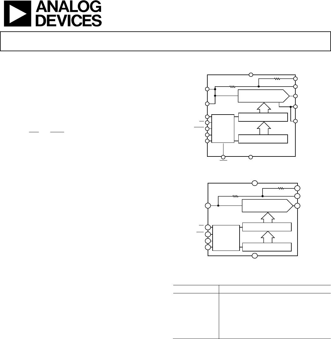
FUNCTIONAL BLOCK DIAGRAM
16-BIT DAC
16-BIT DAC LATCH
V
DD
DGND
LDAC
REFF
V
LOGIC
CS
DIN
CLR
V
OUT
INV
R
FB
AD5512A/
AD5542A
SCLK
R
FB
R
INV
09199-001
REFS
A
GNDF
A
GNDS
CONTROL
LOGIC
SERIAL INPUT REGISTER
Figure 1. 16-Lead TSSOP and 16-Lead LFCSP
5
6
10
9
16-BIT DAC
16-BIT DAC LATCH
SERIAL INPUT REGISTER
GND
V
DD
CLR
REF
CS
DIN
1
2
4
V
OU
T
7
INV
8
R
FB
AD5542A-1
CONTROL
LOGIC
3
SCLK
R
FB
R
INV
09199-002
Figure 2. 10-Lead LFCSP
Table 1. Related Devices
Part No. Description
AD5040/AD5060 2.7 V to 5.5 V 14-/16-bit buffed output DACs
AD5541/AD5542
2.7 V to 5.5 V 16-bit voltage output DACs
AD5781/AD5791
18-
/
20-bit voltage output DACs
AD5570
16-bit ±12 V/±15 V bipolar output DAC
AD5024/AD5064
4.5 V to 5.5 V, 12-
/
16-bit quad channel DAC
AD5764 16-bit, bipolar, voltage output DAC
PRODUCT HIGHLIGHTS
1. 16-bit performance without adjustment.
2. 2.7 V to 5.5 V single supply operation.
3. Low 11.8 nV/√Hz noise spectral density.
4. Low 0.05 ppm/°C temperature drift.
5. 3 mm × 3 mm LFCSP and TSSOP packaging.
AD5512A/AD5542A Data Sheet
Rev. C | Page 2 of 21
TABLE OF CONTENTS
Features .............................................................................................. 1
Applications ....................................................................................... 1
General Description ......................................................................... 1
Functional Block Diagram .............................................................. 1
Product Highlights ........................................................................... 1
Revision History ............................................................................... 2
Specifications ..................................................................................... 3
AD5512A ....................................................................................... 3
AD5542A ....................................................................................... 4
AC Characteristics ........................................................................ 5
Timing Characteristics ................................................................ 6
Absolute Maximum Ratings ............................................................ 7
ESD Caution .................................................................................. 7
Pin Configuration and Function Descriptions ............................. 8
Typical Performance Characteristics ........................................... 10
Terminology .................................................................................... 14
Theory of Operation ...................................................................... 15
Digital-to-Analog Section ......................................................... 15
Serial Interface ............................................................................ 15
Unipolar Output Operation ...................................................... 15
Bipolar Output Operation ......................................................... 16
Output Amplifier Selection ....................................................... 17
Force Sense Amplifier Selection ............................................... 17
Reference and Ground ............................................................... 17
Power-On Reset .......................................................................... 17
Power Supply and Reference Bypassing .................................. 17
Applications Information .............................................................. 18
Microprocessor Interfacing ....................................................... 18
AD5512A/AD5542A to ADSP-BF531 Interface .................... 18
AD5512A/AD5542A to SPORT Interface .............................. 18
AD5512A/AD5542A to 68HC11/68L11 Interface ................... 18
AD5512A/AD5542A to MICROWIRE Interface .................. 18
Layout Guidelines....................................................................... 19
Galvanically Isolated Interface ................................................. 19
Decoding Multiple DACs .......................................................... 19
Outline Dimensions ....................................................................... 20
Ordering Guide .......................................................................... 21
REVISION HISTORY
2/2017—Rev. B to Rev. C
Changes to Figure 4 and Table 7 ..................................................... 8
4/2015—Rev. A to Rev. B
Changes to Power-On Reset Section ............................................ 17
Deleted AD5512A/AD5542A to ADSP-2101 Interface Section .. 18
Updated Outline Dimensions ....................................................... 20
Changes to Ordering Guide .......................................................... 21
5/2011—Rev. 0 to Rev. A
Changes to Table 3, Power Dissipation Value and Endnote 1 .... 4
Changes to Table 5 ............................................................................ 6
Changes to Ordering Guide .......................................................... 21
10/2010—Revision 0: Initial Version
Data Sheet AD5512A/AD5542A
Rev. C | Page 3 of 21
SPECIFICATIONS
AD5512A
V
DD
= 2.7 V to 5.5 V, V
LOGIC
= 2.7 V to 5.5 V, V
REF
= 2.5 V, AGND = DGND = 0 V, −40°C < T
A
< +125°C, unless otherwise noted.
Table 2.
Parameter
1
Min Typ Max Unit Test Condition
STATIC PERFORMANCE
Resolution 12 Bits
Relative Accuracy (INL) ±0.5 ±1.0 LSB
Differential Nonlinearity (DNL)
±0.5
±1.0
Guaranteed monotonic
Gain Error +0.5 ±2 LSB
Gain Error Temperature Coefficient ±0.1 ppm/°C
Unipolar Zero-Code Error 0.03 ±0.5 LSB
Unipolar Zero-Code Temperature Coefficient ±0.05 ppm/°C
Bipolar Resistor Matching 1 Ω/Ω R
FB
/R
INV
, typically R
FB
= R
INV
= 28 kΩ
±0.02
±0.08
% Ratio error
Bipolar Zero Offset Error ±0.07 ±2 LSB
Bipolar Zero Temperature Coefficient ±0.2 ppm/°C
Bipolar Zero-Code Offset Error ±0.02 ±0.5 LSB
Bipolar Gain Error ±0.07 ±2 LSB
Bipolar Gain Temperature Coefficient ±0.1 ppm/°C
OUTPUT CHARACTERISTICS
Output Voltage Range 0 V
REF
− 1 LSB V Unipolar operation
−V
REF
+V
REF
− 1 LSB V Bipolar operation
DAC Output Impedance
6.25
Tolerance typically 20%
Power Supply Rejection Ratio ±1.0 LSB ΔV
DD
± 10%
Output Noise Spectral Density 11.8 nV/√Hz
DAC code = 0x840 (AD5512A) or
0x8400 (AD5542A), frequency = 1 kHz,
unipolar mode
Output Noise 0.134 μV p-p 0.1 Hz to 10 Hz, unipolar mode
DAC REFERENCE INPUT
2
Reference Input Range 2.0 V
DD
V
Reference Input Resistance
3
9
Unipolar operation
7.5 kΩ Bipolar operation
Reference Input Capacitance 26 pF Code 0x0000
26 pF Code 0x3FFF
LOGIC INPUTS
Input Current ±1 μA
Input Low Voltage, V
INL
0.8 V V
DD
= 2.7 V to 5.5 V
Input High Voltage, V
INH
2.4 V V
DD
= 2.7 V to 5.5 V
Input Capacitance
2
10 pF
Hysteresis Voltage
2
0.15
POWER REQUIREMENTS
V
DD
2.7
5.5
All digital inputs at 0 V, V
LOGIC
, or V
DD
I
DD
125 150 µA V
IH
= V
LOGIC
or V
DD
and V
IL
= GND
V
LOGIC
1.8 5.5 V
I
LOGIC
15 24 µA All digital inputs at 0 V, V
LOGIC
, or V
DD
Power Dissipation 1.5 6.05 mW
1
Temperatures are as follows: A version −40°C to +125°C.
2
Guaranteed by design, not subject to production test.
3
Reference input resistance is code-dependent, minimum at 0x855.

AD5542ABCPZ-1-RL7

Mfr. #:
Manufacturer:
Analog Devices Inc.
Description:
Digital to Analog Converters - DAC 16b 2LSB 2.7-5.5V w/ CLR Vlogic
Lifecycle:
New from this manufacturer.
Delivery:
DHL FedEx Ups TNT EMS
Payment:
T/T Paypal Visa MoneyGram Western Union