AD5512A/AD5542A Data Sheet
Rev. C | Page 16 of 21
Assuming a perfect reference, the unipolar worst-case output
voltage can be calculated from the following equation:

INLVVV
D
V
ZSE
GE
REF
N
UNIOUT
2
where:
V
OUT−UNI
is the unipolar mode worst-case output.
D is the code loaded to DAC.
N is the resolution of the DAC.
V
REF
is the reference voltage applied to the part.
V
GE
is the gain error in volts.
V
ZSE
is the zero-scale error in volts.
INL is the integral nonlinearity in volts.
BIPOLAR OUTPUT OPERATION
With the aid of an external op amp, the AD5512A/AD5542A
can be configured to provide a bipolar voltage output. A typical
circuit is shown in Figure 32. The matched bipolar offset resistors,
R
FB
and R
INV
, are connected to an external op amp to achieve
this bipolar output swing, typically R
FB
= R
INV
= 28 kΩ. Table 10
shows the transfer function for this output operating mode.
Also provided on the AD5542A are a set of Kelvin connections
to the analog ground inputs. The example includes the ADR421
2.5 V reference and the AD8628 low offset and zero-drift
reference buffer.
Table 10. AD5542A Bipolar Code Table
DAC Latch Contents
MSB LSB Analog Output
1111 1111 1111 1111 +V
REF
× (32,767/32,768)
1000 0000 0000 0001 +V
REF
× (1/32,768)
1000 0000 0000 0000 0 V
0111 1111 1111 1111 −V
REF
× (1/32,768)
0000 0000 0000 0000 −V
REF
× (32,768/32,768) = −V
REF
Assuming a perfect reference, the worst-case bipolar output
voltage can be calculated from the following equation:
A
RD
RDVRDVV
V
REF
OS
UNIOUT
BIPOUT
)2(1
)]1()2)([(
where:
V
OUT−BIP
is the bipolar mode worst-case output
V
OUT−UNI
is the unipolar mode worst-case output.
V
OS
is the external op amp input offset voltage.
RD is the R
FB
and R
INV
resistor matching error.
A is the op amp open-loop gain.
V
OUT
REFSREFF
INV
R
FB
R
INV
DGND AGNDF
V
DD
DIN
SCLK
LDAC
CS
AD5512A/
AD5542A
AGNDS
+
0.1µF0.1µF
10µF
BIPOLAR
OUTPUT
EXTERNAL
OP AMP
+2.5
V
+5
V
+5V
–5V
SERIAL
INTERFACE
R
FB
09199-024
Figure 32. Bipolar Output
Data Sheet AD5512A/AD5542A
Rev. C | Page 17 of 21
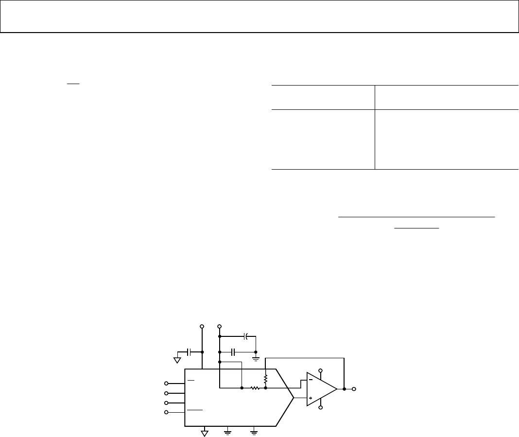
OUTPUT AMPLIFIER SELECTION
For bipolar mode, a precision amplifier should be used and
supplied from a dual power supply. This provides the ±V
REF
output. In a single-supply application, selection of a suitable op
amp may be more difficult because the output swing of the ampli-
fier does not usually include the negative rail, in this case,
AGND. This can result in some degradation of the specified
performance unless the application does not use codes near zero.
The selected op amp must have a very low-offset voltage (the
DAC LSB is 38 μV for the AD5542A with a 2.5 V reference)
to eliminate the need for output offset trims. Input bias current
should also be very low because the bias current, multiplied by
the DAC output impedance (approximately 6 kΩ), adds to the
zero-code error. Rail-to-rail input and output performance is
required. For fast settling, the slew rate of the op amp should
not impede the settling time of the DAC. Output impedance
of the DAC is constant and code-independent, but to minimize
gain errors, the input impedance of the output amplifier should
be as high as possible. The amplifier should also have a 3 dB
bandwidth of 1 MHz or greater. The amplifier adds another
time constant to the system, thus increasing the settling time
of the output. A higher 3 dB amplifier bandwidth results in a
shorter effective settling time of the combined DAC and amplifier.
FORCE SENSE AMPLIFIER SELECTION
Use single-supply, low-noise amplifiers. A low-output impedance
at high frequencies is preferred because the amplifiers must be
able to handle dynamic currents of up to ±20 mA.
REFERENCE AND GROUND
Because the input impedance is code-dependent, the refer-
ence pin should be driven from a low impedance source. The
AD5512A/AD5542A operate with a voltage reference ranging
from 2 V to V
DD
. References below 2 V result in reduced accuracy.
The full-scale output voltage of the DAC is determined by the
reference. Table 9 and Table 10 outline the analog output voltage
or particular digital codes. For optimum performance, Kelvin
sense connections are provided on the AD5512A/AD5542A.
If the application doesn’t require separate force and sense lines,
tie the lines close to the package to minimize voltage drops
between the package leads and the internal die.
POWER-ON RESET
The AD5512A/AD5542A have a power-on reset function to
ensure that the output is at a known state on power-up. On
power-up, the DAC register MSB is 1 and all other bits are 0
until the data is loaded from the serial register. However, the
serial register is not cleared on power-up; therefore, its contents
are undefined. When loading data initially to the DAC, 16 bits or
more should be loaded to prevent erroneous data appearing on
the output. If more than 16 bits are loaded, the last 16 are kept,
and if less than 16 bits are loaded, bits remain from the previous
word. If the AD5512A/AD5542A must be interfaced with data
shorter than 16 bits, the data should be padded with 0s at the
LSBs.
POWER SUPPLY AND REFERENCE BYPASSING
For accurate high-resolution performance, it is recommended
that the reference and supply pins be bypassed with a 10 μF
tantalum capacitor in parallel with a 0.1 μF ceramic capacitor.
AD5512A/AD5542A Data Sheet
Rev. C | Page 18 of 21
APPLICATIONS INFORMATION
MICROPROCESSOR INTERFACING
Microprocessor interfacing to the AD5512A/AD5542A is via
a serial bus that uses standard protocol that is compatible with
DSP processors and microcontrollers. The communications
channel requires a 3- or 4-wire interface consisting of a clock
signal, a data signal, and a synchronization signal. The
AD5512A/AD5542A require a 16-bit data-word with data
valid on the rising edge of SCLK. The DAC update can be
done automatically when all the data is clocked in, or it can
be done under the control of the
LDAC
.
AD5512A/AD5542A TO ADSP-BF531 INTERFACE
The SPI interface of the AD5512A/AD5542A is designed to be
easily connected to industry-standard DSPs and micro-
controllers. Figure 33 shows how the AD5512A/AD5542A
can be connected to the Analog Devices, Inc., Blackfin® DS P.
The Blackfin has an integrated SPI port that can be connected
directly to the SPI pins of the AD5512A/AD5542A.
AD5512A/
AD5542A
CS
SCLK
DIN
LDAC
SPISELx
SCK
MOSI
PF9
ADSP-BF531
09199-044
Figure 33. AD5512A/AD5542A to ADSP-BF531 Interface
AD5512A/AD5542A TO SPORT INTERFACE
The Analog Devices ADSP-BF527 has one SPORT serial port.
Figure 34 shows how one SPORT interface can be used to
control the AD5512A/AD5542A.
09919-045
AD5512A/
AD5542A
CS
SCLK
DIN
LDAC
SPORT_TFS
SPORT_TSCK
SPORT_DT
O
GPIO0
ADSP-BF527
Figure 34. AD5512A/AD5542A to ADSP-BF527 Interface
AD5512A/AD5542A TO 68HC11/68L11 INTERFACE
Figure 35 shows a serial interface between the AD5512A/
AD5542A and the 68HC11/68L11 microcontroller. SCK of
the 68HC11/68L11 drives the SCLK of the DAC, and the
MOSI output drives the serial data line serial DIN. The
CS
signal is driven from one of the port lines. The 68HC11/68L11 is
configured for master mode: MSTR = 1, CPOL = 0, and CPHA =
0. Data appearing on the MOSI output is valid on the rising
edge of SCK.
LDAC
CS
DIN
SCLK
PC6
PC7
MOSI
SCK
AD5512A/
AD5542A*
68HC11/
68L11*
*ADDITIONAL PINS OMITTED FOR CLARITY.
09199-026
Figure 35. AD5512A/AD5542A to 68HC11/68L11 Interface
AD5512A/AD5542A TO MICROWIRE INTERFACE
Figure 36 shows an interface between the AD5512A/AD5542A
and any MICROWIRE-compatible device. Serial data is shifted
out on the falling edge of the serial clock and into the AD5512A/
AD5542A on the rising edge of the serial clock. No glue logic
is required because the DAC clocks data into the input shift
register on the rising edge.
DIN
SCLK
SO
SCLK
AD5512A/
AD5542A*
MICROWIRE*
*ADDITIONAL PINS OMITTED FOR CLARITY.
CS
CS
09199-027
Figure 36. AD5512A/AD5542A to MICROWIRE Interface

AD5542ABCPZ-1-RL7

Mfr. #:
Manufacturer:
Analog Devices Inc.
Description:
Digital to Analog Converters - DAC 16b 2LSB 2.7-5.5V w/ CLR Vlogic
Lifecycle:
New from this manufacturer.
Delivery:
DHL FedEx Ups TNT EMS
Payment:
T/T Paypal Visa MoneyGram Western Union