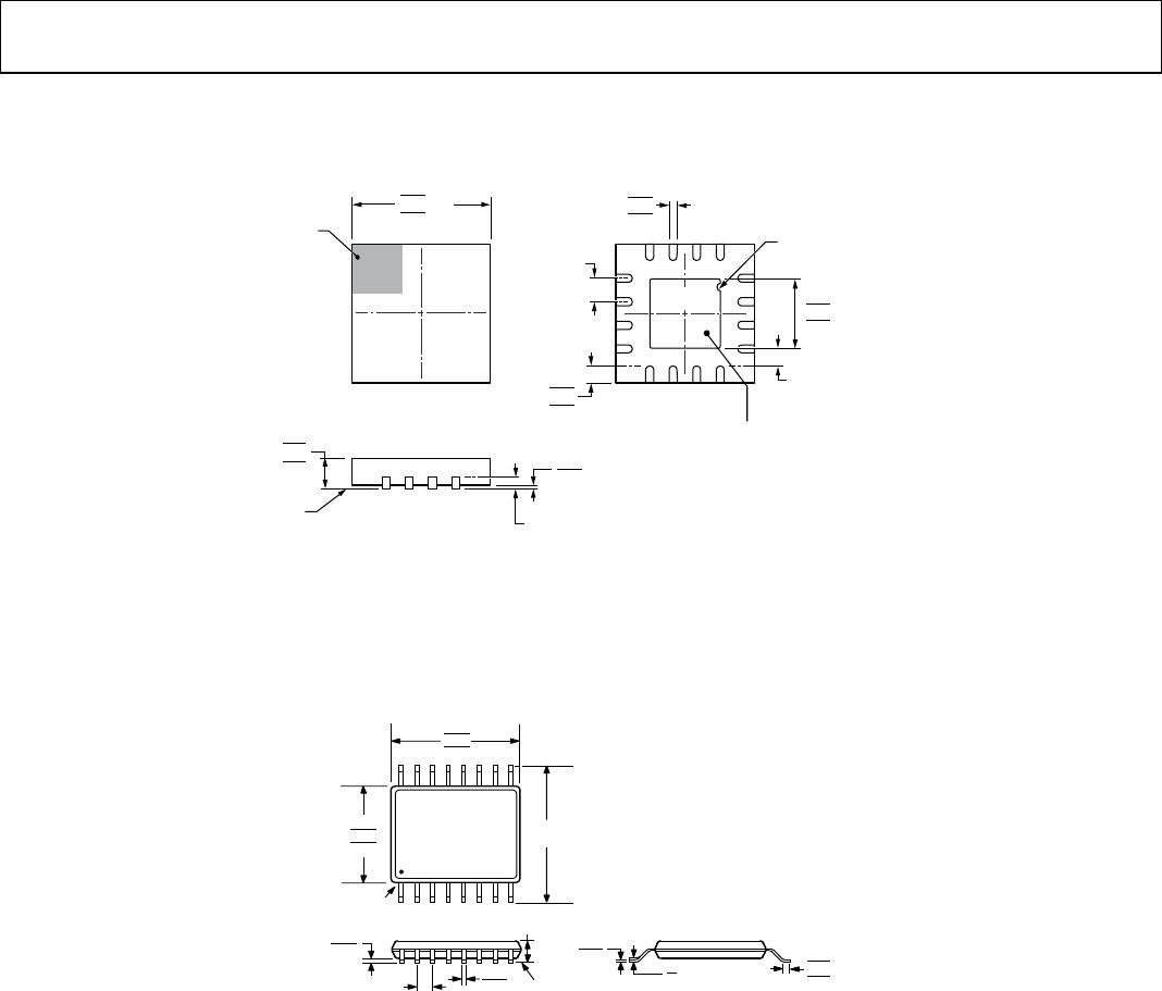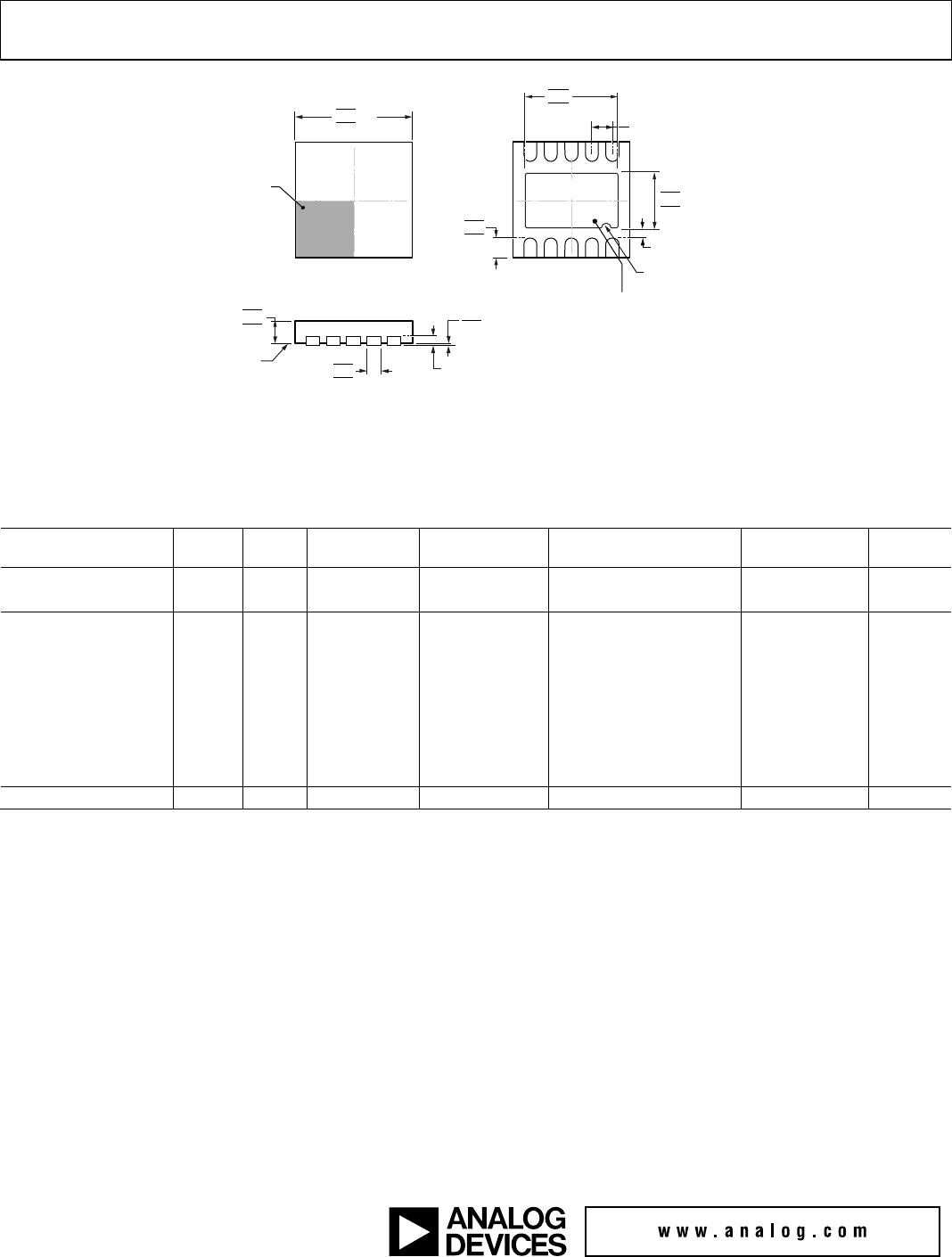
Data Sheet AD5512A/AD5542A
Rev. C | Page 19 of 21
LAYOUT GUIDELINES
In any circuit where accuracy is important, careful consider-
ation of the power supply and ground return layout helps to
ensure the rated performance. Design the printed circuit board
(PCB) on which the AD5512A/AD5542A is mounted so that
the analog and digital sections are separated and confined to
certain areas of the board. If the AD5512A/AD5542A are in a
system where multiple devices require an analog ground-to-
digital ground connection, make the connection at one point
only. Establish the star ground point as close as possible to the
device.
The AD5512A/AD5542A should have ample supply bypassing
of 10 μF in parallel with 0.1 μF on each supply located as close
to the package as possible, ideally right up against the device.
The 10 μF capacitors are the tantalum bead type. The 0.1 μF
capacitor should have low effective series resistance (ESR)
and low effective series inductance (ESI), such as the common
ceramic types, which provide a low impedance path to ground
at high frequencies to handle transient currents due to internal
logic switching.
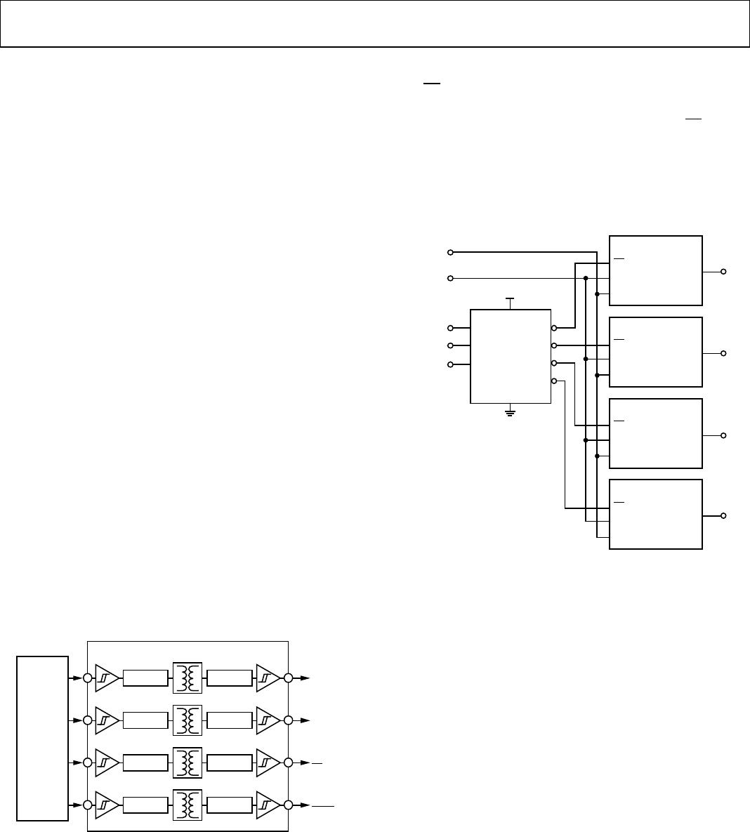
GALVANICALLY ISOLATED INTERFACE
In many process control applications, it is necessary to provide
an isolation barrier between the controller and the unit being
controlled to protect and isolate the controlling circuitry
from any hazardous common-mode voltages that may occur.
iCoupler® products from Analog Devices provide voltage
isolation in excess of 2.5 kV. The serial loading structure
of the AD5512A/AD5542A makes the parts ideal for isolated
interfaces because the number of interface lines is kept to a
minimum. Figure 37 shows a 4-channel isolated interface to
the AD5512A/AD5542A using an ADuM1400. For further
information, visit http://www.analog.com/icouplers.
ENCODE
SERIA
L
CLOCK IN
CONTROLLER
ADuM1400
1
SERIAL
D
ATA OUT
SYNC OUT
LOAD DAC
OUT
DECODE
TO
SCLK
T
O
DIN
TO
CS
TO
LDAC
V
IA
V
O
A
ENCODE
DECODE
V
IB
V
OB
ENCODE DECODE
V
IC
V
OC
ENCODE DECODE
V
ID
V
OD
1
ADDITIONA
L PINS OMITTED FOR CLARIT
Y.
09199-046
Figure 37. Isolated Interface
DECODING MULTIPLE DACS
The
CS
pin of the AD5512A/AD5542A can be used to select
one of a number of DACs. All devices receive the same serial
clock and serial data, but only one device receives the
CS
signal
at any one time. The DAC addressed is determined by the
decoder. There is some digital feedthrough from the digital
input lines. Using a burst clock minimizes the effects of digital
feedthrough on the analog signal channels. Figure 38 shows a
typical circuit.
AD5512A/
AD5542A
CS
DIN
SCLK
V
OUT
AD5512A/
AD5542A
CS
DIN
SCLK
V
OUT
AD5512A/
AD5542A
CS
DIN
SCLK
V
OUT
AD5512A/
AD5542A
CS
DIN
SCLK
V
OUT
V
DD
DGND
EN
CODED
ADDRESS
SCLK
DIN
ENABLE
DECODER
09199-030
Figure 38. Addressing Multiple DACs