© Semtech 2006 www.semtech.com
23
XE1202A TrueRF™
5.2.6 Supplementary configuration
Configuration settings to optimize device performance under certain operation conditions are described in Table 19
below:
Name
Bits Byte Address
Description
TParam_BW
2 10011
Bandwidth decoding map:
Baseband filter bandwidth
(RTParam_BW):
0 -> default values:
RTParam_BW(1:0) = 00 => 10 kHz
RTParam_BW(1:0) = 01 => 20 kHz
RTParam_BW(1:0) = 10 => 40 kHz
RTParam_BW(1:0) = 11 => 200 kHz
1 -> new values:
RTParam_BW(1:0) = 00 => 14.3 kHz
RTParam_BW(1:0) = 01 => 28.5 kHz
RTParam_BW(1:0) = 10 => 66.7 kHz
RTParam_BW(1:0) = 11 => 100 kHz
TParam_HPF
5-3 10110
Cut-off frequency of the HPF stages
allowing to cancel the DC and low-
frequency offsets in the baseband
circuit:
0 0 0 -> 660 Hz (default value)
0 0 1 -> 1.48 kHz
0 1 0 -> 1.75 kHz
0 1 1 -> 1.96 kHz
1 0 0 -> 2.55 kHz
1 0 1 -> 3.34 kHz
1 1 0 -> 5.11 kHz
1 1 1 -> 10.2 kHz
Table 19: Supplementary configuration
Using TParam_BW allows intermediate bandwidths to be accessed; these additional bandwidths can be selected to
optimize the sensitivity and the selectivity of the applications for which the signal bandwidth is different from the 4
default filter bandwidths.
The wake-up time of the receiver may be reduced by increasing the cut-off frequency of the HPF stages. This is
accomplished by changing the value of TParam_HPF.
Note that the selected cut-off frequency should be less than (f – (BR/2)) to avoid sensitivity degradation.
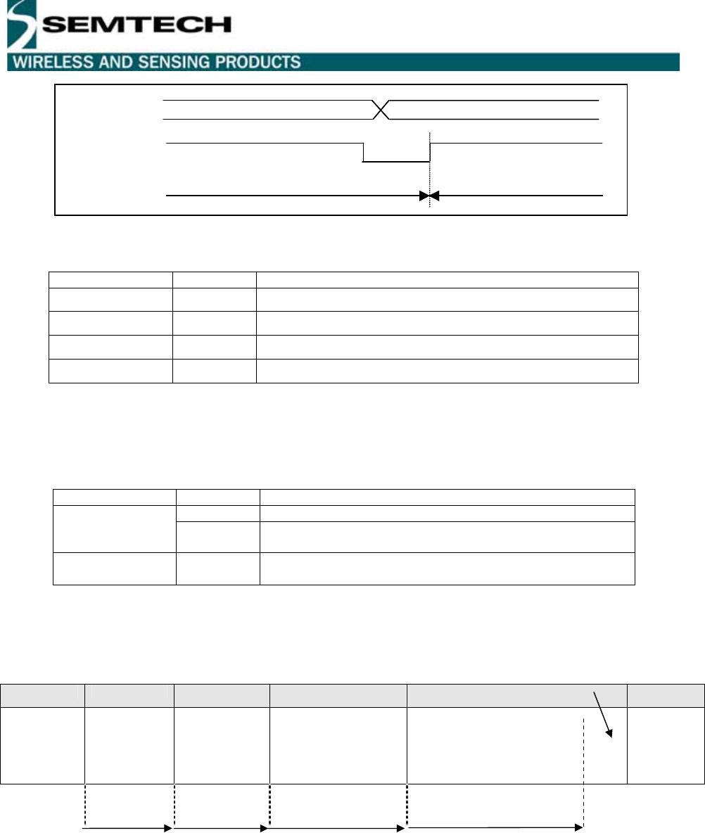
5.3 Operating Modes
The XE1202A TrueRF™ has 4 main operating modes as set by the MODE[2:0] inputs as illustrated in Table 20
below. Switching between modes is only possible when the /EN signal is low. The actual change will be applied to
the transceiver upon the rising edge of the /EN signal.
Over the operating supply and temperature range, set-up and hold time for MODE[2:0] on the rising edge of /EN is
200 ns, while the negative pulse duration on /EN is 2 µs minimum. Please refer to Figure 9:
© Semtech 2006 www.semtech.com
24
XE1202A TrueRF™
Name MODE(2:0) Description
Sleep mode
0 0 0 -
Standby mode
0 0 1 Xtal oscillator enabled
Receiver mode
1 0 0 Xtal oscillator, Frequency synthesizer, Receiver enabled
Transmitter mode
1 1 1 Xtal oscillator, Frequency synthesizer, Transmitter enabled
Table 20: XE1202A Main operating modes
Three additional operating modes are defined and should be used when the transceiver is switched from the
standby mode to the receiver or transmitter mode. These additional operating modes are illustrated in Table 21
below.
Name MODE(2:0) Description
0 1 0 Xtal oscillator, Baseband enabled (first step)
Receiver mode
0 1 1 Xtal oscillator, Frequency synthesizer, Baseband enabled
(first step)
Transmitter mode
1 1 0 Xtal oscillator, Frequency synthesizer enabled
Table 21: XE1202A Additional operating modes
The power up sequence from sleep to receiver mode is selected by setting the RTParam_WBB parameter to “0”. The
sequence is described in Table 22 below:
Received data valid
Mode = 000 Mode = 001 Mode = 010 Mode = 011 Mode = 100 Mode=001
- Sleep - Xtal
oscillator
enenabled
- Baseband
- Xtal
oscillator
enabled
- Frequency
synthesizer
- Baseband
- Xtal oscillator
enabled
- RF Front End
- Frequency synthesizer
- Baseband
- Xtal oscillator
enabled
- Xtal
oscillator
enabled
TS_OS TS_BBR TS_FS TS_BB2
Table 22: Power up sequence from Standby to Receive Mode
XXX
MODE[2:0]
EN
YXY
Transceiver in Mode XXX Transceiver in Mode YXY
XXX
MODE[2:0]
EN
YXY
Transceiver in Mode XXX Transceiver in Mode YXY
Figure 9: Switching mode sequence
© Semtech 2006 www.semtech.com
25
XE1202A TrueRF™
The typical current consumption values during the power-up sequence from Standby to Receive Mode are shown
in Table 23 as follows:
14.0 mA
11.5 mA
3.0 mA
0.85 mA
<1 uA
Mode= 000 Mode= 001 Mode=010 Mode =011 Mode = 100
TS_OS TS_BBR TS_FS TS_BB2
Table 23: Typical current consumption profile during the power up sequence from Standby to Receive Mode
The power up sequence from sleep to transmit mode is described in Table 24:
Transmission
Mode = 000 Mode = 001 Mode = 110 Mode =111 Mode=001
- Sleep - Xtal
oscillator
enabled
- Frequency
synthesizer
- Xtal
oscillator
enabled
- Power Amplifier
- Frequency synthesizer
- Xtal oscillator
enabled
- Xtal
oscillator
enabled
TS_OS TS_FS TS_TR
Table 24: Standard power up sequence from Standby to Transmit Mode
5.4 Transmitted Data Interface
When in transmit mode (MODE[2:0] = 111), the DATAIN signal is used as input for the on-chip modulator. DATAIN
is not sampled, so the bit duration should match the bit rate setting of the receiver. Whenever XE1202A TrueRF™
are used on both sides of the communication link, the bit rate should be one of those defined in Table 4 (BR). In
this case the bit rate error should be less than 5 % compared to the specified value.
5.5 Received Data Interface
The outputs of the receiver are the two signals DATAOUT and DCLK. When the bit “RTParam_Bits” is “1”, the bit
synchronizer is turned on, and the two output signals are respectively the output NRZ bit stream and the sampling
clock. The value of DATAOUT is valid at the rising edge of DCLK (see Figure 11 on next page):
DATAIN
(NRZ)
BIT N
BIT N+1
1/BR
DATAIN
(NRZ)
BIT N
BIT N+1
1/BR
Figure 10: DATAIN timing

XE1202AI027TRLF

Mfr. #:
Manufacturer:
Semtech
Description:
RF Transceiver XE1202AI027TRLF
Lifecycle:
New from this manufacturer.
Delivery:
DHL FedEx Ups TNT EMS
Payment:
T/T Paypal Visa MoneyGram Western Union

Products related to this Datasheet