© Semtech 2006 www.semtech.com
5
XE1202A TrueRF™
2 Pin Description
PIN NAME DESCRIPTION
1 MODE(1) In Transmit/Receive/Standby/Sleep Mode Select
2 MODE(0) In Transmit/Receive/Standby/Sleep Mode Select
3 /EN In Chip Enable
4 VSSF RF Analog Ground
5 RFA In RF Input
6 RFB In RF Input
7 VSSP In Power Amplifier Ground
8 VSSP In Power Amplifier Ground
9 RFOUT Out RF Output
10 VDDP Power Amplifier Supply Voltage
11 VSSP Power Amplifier Ground
12 VDD RF Analog Supply Voltage
13 TKA I/O VCO Tank
14 TKB I/O VCO Tank
15 VSSF RF Analog Ground
16 LFB I/O PLL Loop Filter
17 VDDD RF Digital Supply Voltage
18 VSSD RF Digital Ground
19 TSUPP Test Circuit Supply Voltage (connected to VSS in normal operation)
20 SCAN In Scan Test Input (connected to VSS in normal operation)
21 OPT (connected to VSS in normal operation)
22 TMOD[0] (connected to VSS in normal operation)
23 TMOD[1] (connected to VSS in normal operation)
24 VSSA Analog Ground
25 XTA I/O Ref Xtal / Input of external clock
26 VSSA Analog Ground
27 XTB I/O Reference Xtal
28 VDDA Analog Supply Voltage
29 QAMP Out Buffered Q Output
30 IAMP Out Buffered I Output
31 TMOD[2] (connected to VSS in normal operation)
32 TMOD[3] (connected to VSS in normal operation)
33 TIBIAS (connected to VSS in normal operation)
34 VDD Digital Supply Voltage
35 SO Out Configuration Register Serial Output
36 SI In Configuration Register Serial Input
37 SCK In Configuration Register Serial Clock
38 CLKOUT Out Output clock at reference frequency divided by 4, 8, 16 or 32
39 VSS Digital Ground
40 DCLK Out Recovered Received Data Clock
41 DATAOUT Out Received Data
42 DATAIN In Transmit Data
43 PATTERN Out Output of the pattern recognition block
44 MODE(2) In Transmit/Receive/Standby/Sleep Mode Select
Table 1: Pin Description
© Semtech 2006 www.semtech.com
6
XE1202A TrueRF™
3 Electrical Characteristics
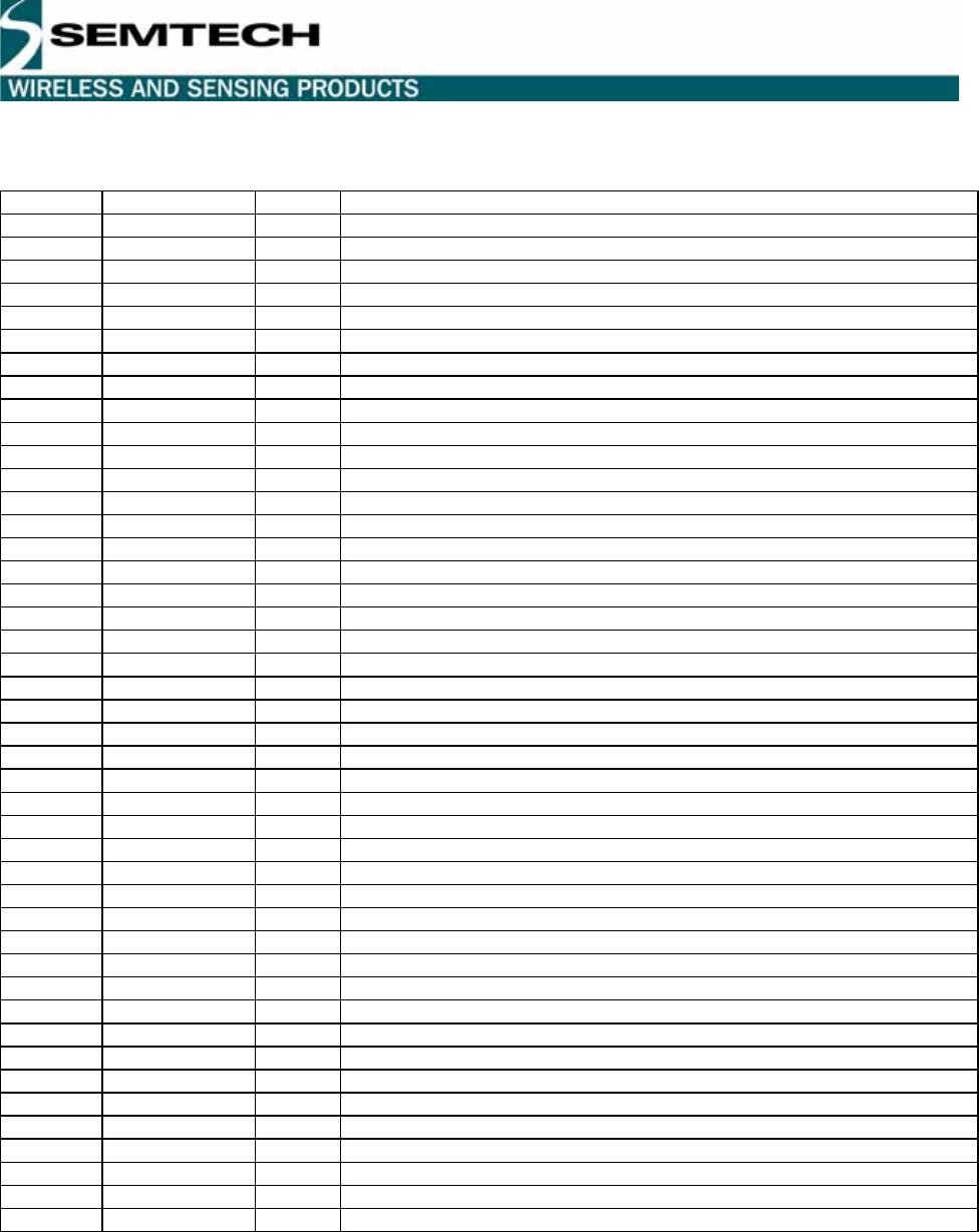
3.1 Absolute Maximum Operating Ranges
Stresses above those values listed below may cause permanent device failure. Exposure to absolute maximum
ratings for extended periods may affect device reliability.
Symbol Description Min. Max. Unit
VDDmax Supply voltage -0.4 3.9 V
ML Receiver input level -5 dBm
Tmax Storage temperature -55 125 °C
Table 2: Absolute Maximum Operating Ranges
The device is ESD sensitive and should be handled with precaution.
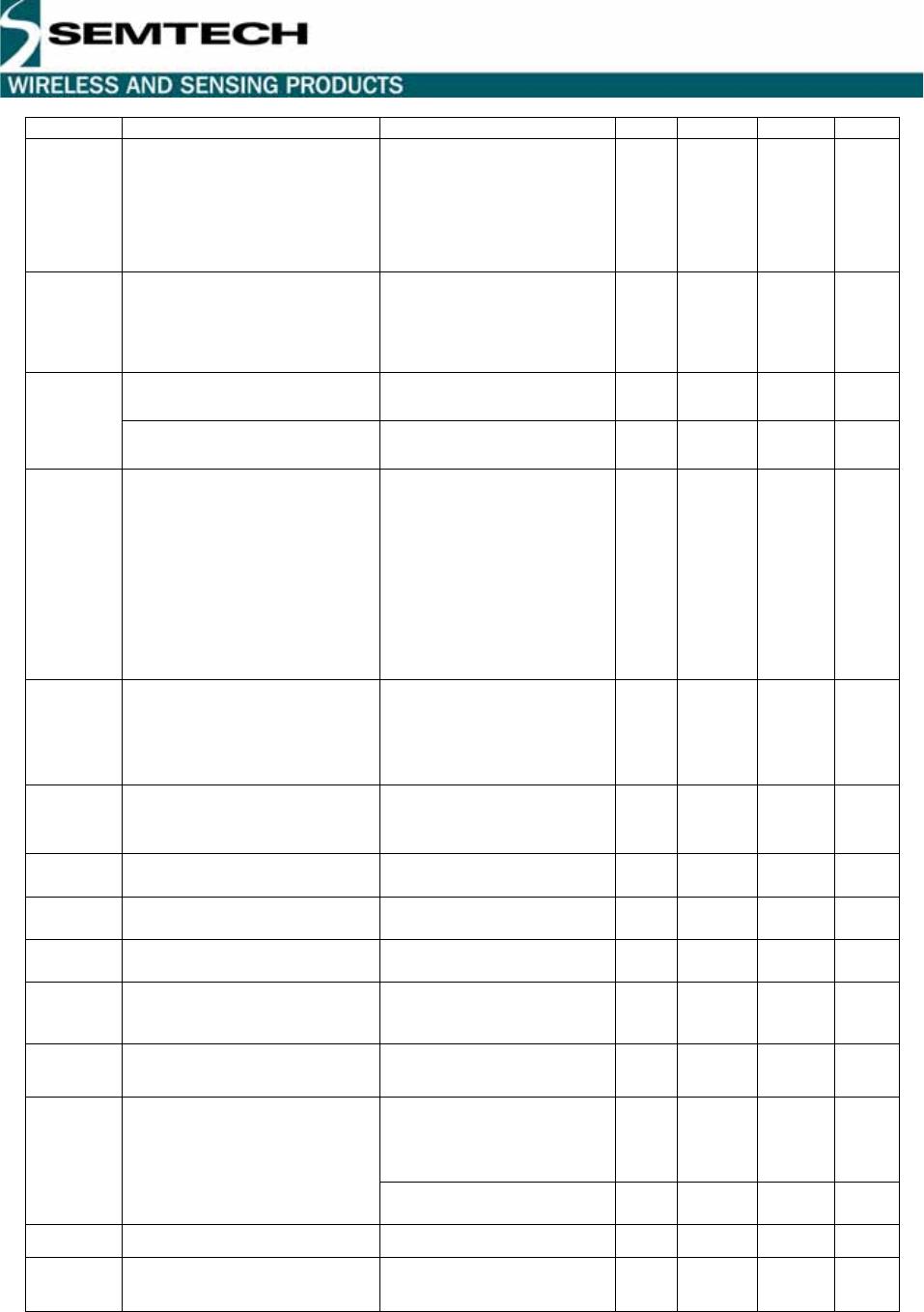
3.2 Specifications
3.2.1 Operating Range
Symbol Description Min. Max. Unit
VDD Supply voltage 2.4 (*) 3.6 V
T Temperature -40 85 °C
CLop Load capacitance on digital ports - 25 pF
Table 3: Operating Range
(*) For narrow-band configurations (base-band filter bandwidths of 10, 20 and 40 kHz), the minimum operating
supply voltage is 2.4 V. For 200 kHz base-band filter bandwidth setting the minimum operating supply voltage is 2.7
V.
3.2.2 Electrical Specifications
The table below gives the electrical specifications of the transceiver under the following conditions:
Supply Voltage = 3.3 V, temperature = 25 °C, 2-level FSK without pre-filtering, f
C
= 434, 869 and 915 MHz,
f = 5 kHz, Bit rate = 4.8 kbits/s, BW
SSB
= 10 kHz, BER = 1 % (measured at the output of the bit synchronizer), LNA
input and PA output matched to 50 , environment as defined in section 6, unless otherwise specified.
Symbol Description Conditions Min Typ Max Unit
IDDSL Supply current in sleep mode - 0.2 1 µA
IDDST Supply current in standby
mode
Crystal oscillator (39 MHz)
enabled
- 0.85 1.10 mA
IDDR Supply current in receive
mode
- 14 16.5 mA
IDDT Supply current in transmitter
mode
RFOP = 5 dBm
RFOP = 15 dBm
-
-
33
62
40
75
mA
mA
RF sensitivity 869 / 915 MHz A-mode
B-mode
- -116
-103
-113
-100
dBm
dBm
RFS
RF sensitivity 434 MHz A-mode
B-mode
- -114
-100
-111
-98
dBm
dBm
FDA Frequency deviation
Programmable
-
-
-
-
-
5
10
20
40
100
-
-
-
-
-
kHz
kHz
kHz
kHz
kHz
CCR Co-channel rejection -13 -10 - dBc
© Semtech 2006 www.semtech.com
7
XE1202A TrueRF™
Symbol Description Conditions Min Typ Max Unit
IIP3
Input intercept point (from
LNA input to base-band filter
output)
f
1
= f
LO
+ 1 MHz,
f
2
= f
LO
+ 1.995 MHz
A-mode
B-mode
-36
-21
-33
-18
-
-
dBm
dBm
BW Base band filter bandwidth Programmable -
-
-
-
10
20
40
200
-
-
-
-
kHz
kHz
kHz
kHz
Adjacent channel rejection
869 / 915 MHz
funw = f
LO
+ 65 kHz
Pw=-107 dBm, A-mode
45 48
-
dBc ACR
Adjacent channel rejection
434 MHz
funw = f
LO
+ 65 kHz
Pw=-102 dBm, A-mode
42 45
-
dBc
BR
Bit rate Programmable
-
-
-
-
-
4.8
9.6
19.2
38.4
76.8
-
-
-
-
-
kbits/
s
kbits/
s
kbits/
s
kbits/
s
kbits/
s
RFOP RF output power Programmable
RFOP1
RFOP2
RFOP3
RFOP4
-3
+2
+7
+12
0
+5
+10
+15
-
-
-
-
dBm
dBm
dBm
dBm
FR Synthesizer frequency range Programmable
Each range with its own
external components
433
868
902
-
-
-
435
870
928
MHz
MHz
MHz
TS_BBR Receiver baseband wake-up
time (first step)
Crystal oscillator enabled
- 200 250 µs
TS_TR Transmitter wake-up time Frequency synthesizer
enabled
- 100 150 µs
TS_FS Frequency synthesizer wake-
up time
Crystal oscillator enabled - 200 250 µs
TS_BB2
Receiver RF Front-End
wake-up time
Frequency synthesizer
enabled
RTParam_WBB=0
- 500 600 µs
TS_FSW
Frequency synthesizer
switching time
Between 2 channels at 1
MHz channel spacing
100 150 µs
RSSI enabled during
mode 010 0.5 ms before
switching to mode 100
(see figure 8)
- - 1.0 ms
TS_RS
RSSI wake-up time (receiver
operation in mode 100)
RSSI enabled during
mode 100
- - 1.5 ms
TS_RSM
RSSI measurement time
- 0.5 - ms
TS_OS
Crystal oscillator wake-up
time
- 0.3 0.5 ms

XE1202AI027TRLF

Mfr. #:
Manufacturer:
Semtech
Description:
RF Transceiver XE1202AI027TRLF
Lifecycle:
New from this manufacturer.
Delivery:
DHL FedEx Ups TNT EMS
Payment:
T/T Paypal Visa MoneyGram Western Union

Products related to this Datasheet