LTC4000
12
4000fb
For more information www.linear.com/LTC4000
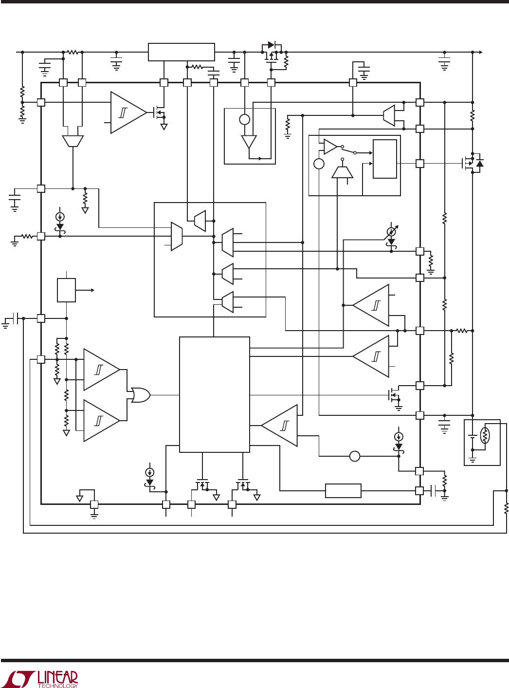
operaTion
Overview
The LTC4000 is designed to simplify the conversion of
any externally compensated DC/DC converter into a high
performance battery charger with PowerPath control. It
only requires the DC/DC converter to have a control or
external-compensation pin (usually named VC or ITH)
whose voltage level varies in a positive monotonic way
with its output. The output variable can be either output
voltage or output current. For the following discussion,
refer to the Block Diagram in Figure 1.
The LTC4000 includes four different regulation loops: input
current, charge current, battery float voltage and output
voltage (A4-A7). Whichever loop requires the lowest volt-
age on the ITH pin for its regulation controls the external
DC/DC converter.
The input current regulation loop ensures that the pro-
grammed input current limit (using a resistor at IL) is not
exceeded at steady state. The charge current regulation
loop ensures that the programmed battery charge current
limit (using a resistor at CL) is not exceeded. The float volt-
age regulation loop ensures that the programmed battery
stack voltage (using a resistor divider from BAT to FBG
via BFB) is not exceeded. The output voltage regulation
loop ensures that the programmed
system output voltage
(using
a resistor divider from CSP to FBG via OFB) is not
exceeded. The LTC4000 also provides monitoring pins
for the input current and charge current at the IIMON and
IBMON pins respectively.
The LTC4000 features an ideal diode controller at the input
from the IID pin to the CSP pin and a PowerPath controller
at the output from the BAT pin to the CSN pin. The output
PowerPath controller behaves as an ideal diode controller
when not charging. When charging, the output PowerPath
controller has two modes of operation. If V
OFB
is greater
than V
OUT(INST_ON)
, BGATE is driven low. When V
OFB
is
less than V
OUT(INST_ON)
, a linear regulator implements
the instant-on feature. This feature provides regulation of
the BGATE pin so that a valid voltage level is immediately
available at the output when the LTC4000 is charging an
over-discharged, dead or short faulted battery.
The state of the ENC pin determines whether charging is
enabled. When ENC is grounded, charging is disabled and
the battery float voltage loop is disabled. Charging is enabled
when the ENC pin is left floating or pulled high (≥1.5V)
The
LTC4000 offers several user configurable battery
charge termination schemes. The TMR pin can be config-
ured for either C/X termination, charge timer termination or
no termination. After a particular charge cycle terminates,
the LTC4000 features an automatic recharge cycle if the
battery voltage drops below 97.6% of the programmed
float voltage.
Trickle charge mode drops the charge current to one
tenth of the normal charge current (programmed using a
resistor from the CL pin to GND) when charging into an
over discharged or dead battery. When trickle charging,
a capacitor on the TMR pin can be used to program a
time out period. When this bad battery timer expires and
the battery voltage fails to charge above the low battery
threshold (V
LOBAT
), the LTC4000 will terminate charging
and indicate a bad battery condition through the status
pins (F LT and CHRG).
The LTC4000 also includes an NTC pin, which provides
temperature qualified charging when connected to an NTC
thermistor thermally coupled to the battery pack. To enable
this feature, connect the thermistor between the NTC and
the GND pins, and a corresponding resistor from the BIAS
pin to the NTC pin. The LTC4000 also provides a charging
status
indicator through the F LT and the CHRG pins.
Aside from biasing the thermistor-resistor network, the
BIAS pin can also be used for a convenient pull up voltage.
This pin is the output of a low dropout voltage regulator
that is capable of providing up to 0.5mA of current. The
regulated voltage on the BIAS pin is available as soon as
the IN pin is within its operating range (≥3V).
Input Ideal Diode
The input ideal diode feature provides low loss conduction
and reverse blocking from the IID pin to the CSP pin. This
reverse blocking prevents reverse current from the output
(CSP pin) to the input (IID pin) which causes unneces-
sary drain on the battery and in some cases may result
in unexpected DC/DC converter behavior.
The ideal diode behavior is achieved by controlling an
external PMOS connected to the IID pin (drain) and the