LTC4000
7
4000fb
For more information www.linear.com/LTC4000
Typical perForMance characTerisTics
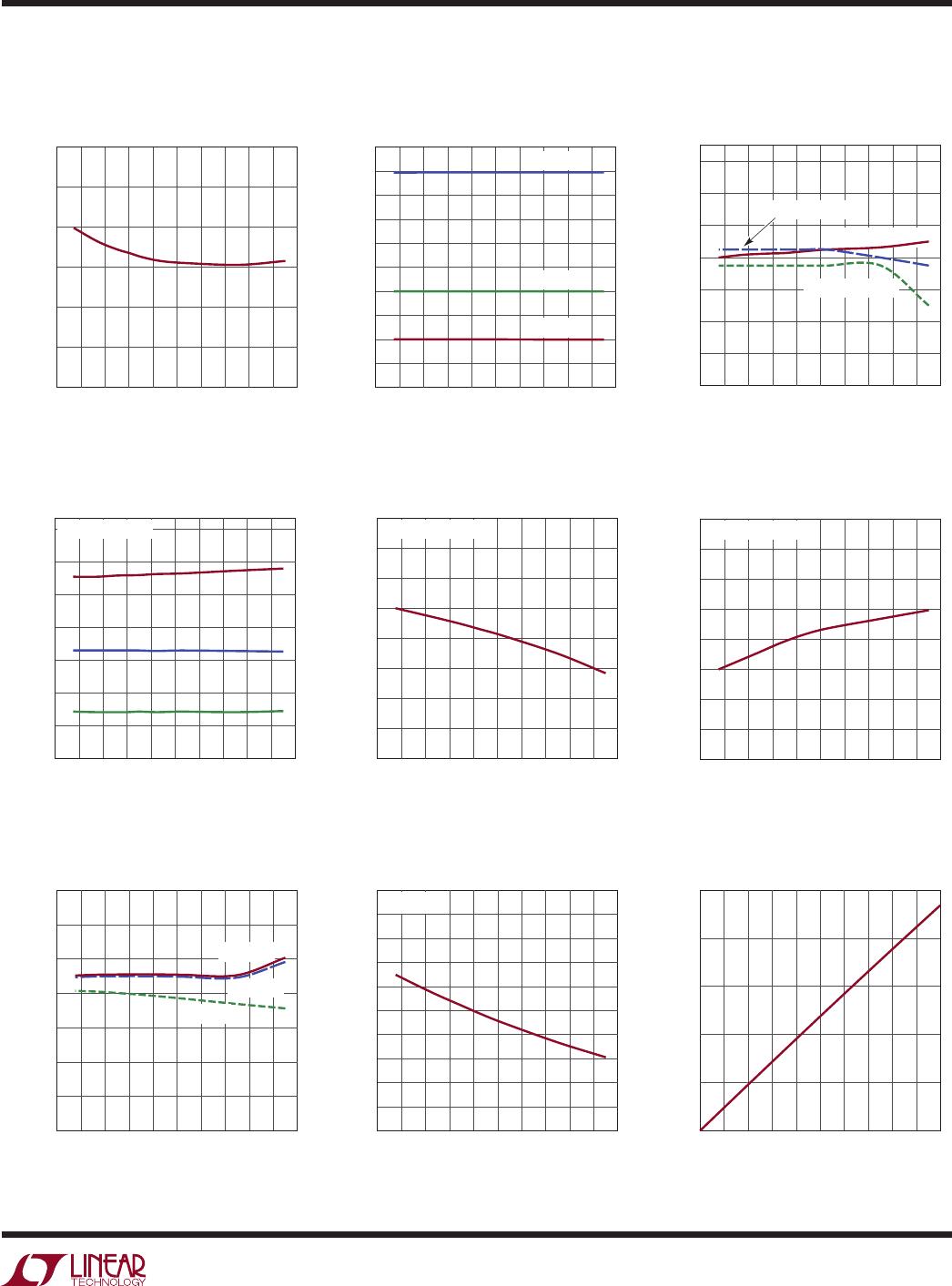
PowerPath Turn-Off Gate Voltage
Over Temperature
BIAS Voltage at 0.5mA Load Over
Temperature
I
TH
Pull-Down Current Over
Temperature
PowerPath Forward Voltage
Regulation Over Temperature
PowerPath Fast Off, Fast On
and Forward Regulation Over
Temperature
PowerPath Turn-On Gate Clamp
Voltage Over Temperature
Charge Termination Time with 0.1µF
Timer Capacitor Over Temperature
NTC Thresholds Over
Temperature
TEMPERATURE (°C)
–60
T
T
(h)
3.5
3.3
3.1
2.9
2.7
2.5
2.3
10020
4000 G10
14040 60 80–20 0–40 120
TEMPERATURE (°C)
–60
PERCENT OF V
BIAS
(%)
80
65
75
70
45
55
60
50
40
35
30
10020
4000 G11
14040 60 80–20 0–40 120
V
NTC(OPEN)
V
NTC(HOT)
V
NTC(COLD)
TEMPERATURE (°C)
–60
V
IID,CSP
/V
BAT,CSN
(mV)
14
6
10
12
8
4
2
0
10020
4000 G12
14040 60 80–20 0–40 120
V
IID
= V
BAT
= 60V
V
IID
= V
BAT
= 3V
V
IID
= V
BAT
= 15V
TEMPERATURE (°C)
–60
V
IID,CSP
/V
BAT,CSN
(mV)
120
0
60
90
30
–30
–60
–90
10020
4000 G13
14040 60 80–20 0–40 120
V
IID
= V
BAT
= 15V
TEMPERATURE (°C)
–60
IGATE (ON)
BGATE(ON)
12.5
13.5
14.5
14.0
13.0
12.0
11.5
11.0
10020
4000 G14
14040 60 80–20 0–40 120
V
IID
= V
BAT
= 15V
TEMPERATURE (°C)
–60
V
MAX(IID,CSP),IGATE
/V
MAX(BAT,CSN),BGATE
(mV)
350
450
550
500
400
300
250
200
10020
4000 G15
14040 60 80–20 0–40 120
V
CSP
= V
CSN
= 15V
TEMPERATURE (°C)
–60
BIAS
2.8
3.0
3.1
2.9
2.7
2.6
2.5
10020
4000 G16
14040 60 80–20 0–40 120
V
IN
= 60V
V
IN
= 15V
V
IN
= 3V
TEMPERATURE (°C)
–60
I
ITH(PULL-DOWN)
(mA)
1.5
0.8
1.0
1.1
1.2
1.3
1.4
0.9
0.7
0.6
0.5
10020
4000 G17
14040 60 80–20 0–40 120
V
ITH
= 0.4V
I
TH
Pull-Down Current
vs V
ITH
V
ITH
(V)
0
I
ITH(PULL-DOWN)
(mA)
2.5
1.5
2.0
1.0
0.5
0
0.80.4
4000 G18
10.5 0.6 0.70.2 0.30.1 0.9
LTC4000
8
4000fb
For more information www.linear.com/LTC4000
pin FuncTions
VM (Pin 1/Pin 25): Voltage Monitor Input. High impedance
input to an accurate comparator with a 1.193V threshold
(typical). This pin controls the state of the RST output
pin. Connect a resistor divider (R
VM1
, R
VM2
) between the
monitored voltage and GND, with the center tap point con-
nected to this pin. The falling threshold of the monitored
voltage is calculated as follows:
V
VM _RST
=
R
VM1
+R
VM2
R
VM2
1.193V
where R
VM2
is the bottom resistor between the VM pin
and GND. Tie to the BIAS pin if voltage monitoring func-
tion is not used.
RST (Pin 2/Pin 26): High Voltage Open Drain Reset Output.
When the voltage at the VM pin is below 1.193V, this status
pin is pulled low. When driven low, this pin can disable
a DC/DC converter when connected to the converter’s
enable pin. This pin can also drive an LED to provide a
visual status indicator of a monitored voltage. Short this
pin to GND when not used.
IIMON (Pin 3/Pin 27): Input Current Monitor. The voltage
on this pin is 20 times (typical) the sense voltage (V
IN,CLN
)
across the input current sense resistor(R
IS
), therefore
providing a voltage proportional to the input current.
Connect an appropriate capacitor to this pin to obtain a
voltage representation of the time-average input current.
Short this pin to GND to disable input current limit feature.
IL (Pin 4/Pin 28): Input Current Limit Programming. Con-
nect the input current programming resistor (R
IL
) to this
pin. This pin sources 50µA of current. The regulation loop
compares the voltage on this pin with the
input current
monitor
voltage (V
IIMON
), and drives the ITH pin accord-
ingly to ensure that the programmed input current limit is
not exceeded. The input current limit is determined using
the following formula:
I
ILIM
= 2.5µA
R
IL
R
IS
where R
IS
is the sense resistor connected to the IN and
the CLN pins. Leave the pin open for the maximum input
current limit of 50mV/R
IS
.
ENC (Pin 5/Pin 1): Enable Charging Pin. High impedance
digital input pin. Pull this pin above 1.5V to enable charg-
ing and below 0.5V to disable charging. Leaving this pin
open causes the internalA pull-up current to pull the
pin to 2.5V (typical).
IBMON (Pin 6/Pin 2): Battery Charge Current Monitor. The
voltage on this pin is 20 times (typical) the sense voltage
(V
CSP,CSN
) across the battery current sense resistor (R
CS
),
therefore providing a voltage proportional to the battery
charge current. Connect an appropriate capacitor to this
pin to obtain a voltage representation of the time-average
battery charge current. Short this pin to GND to disable
charge current limit feature.
CX (Pin 7/Pin 3): Charge Current Termination Pro-
gramming. Connect the charge current termination pro-
gramming resistor (R
CX
) to this pin. This pin is a high
impedance input to a comparator and sourcesA of
current. When the voltage on this pin is greater than the
charge current monitor voltage (V
IBMON
), the CHRG pin
turns high impedance indicating that the CX threshold is
reached.
When this occurs, the charge current is imme-
diately terminated if the TMR pin is shorted to the BIAS
pin, otherwise charging continues until the charge termi-
nation timer expires. The charge current termination value
is determined using the following formula:
I
C/X
=
0.25µA R
CX
( )
0.5mV
R
CS
Where R
CS
is the sense resistor connected to the CSP
and the CSN pins. Note that if R
CX
= R
CL
≤ 19.1kΩ, where
R
CL
is the charge current programming resistor, then the
charge current termination value is one tenth the full charge
current, more familiarly known as C/10. Short this pin to
GND to disable CX termination.
CL (Pin 8/Pin 4): Charge Current Limit Programming. Con-
nect the charge current programming resistor (R
CL
) to this
pin. This pin sources 50µA of current. The regulation loop
compares the voltage on this pin with the charge current
monitor voltage (V
IBMON
), and drives the ITH pin accord-
ingly to ensure that the programmed charge current limit
(QFN/SSOP)
LTC4000
9
4000fb
For more information www.linear.com/LTC4000
pin FuncTions
(QFN/SSOP)
is not exceeded. The charge current limit is determined
using the following formula:
I
CLIM
= 2.5µA
R
CL
R
CS
Where R
CS
is the sense resistor connected to the CSP
and the CSN pins. Leave the pin open for the maximum
charge current limit of 50mV/R
CS
.
TMR (Pin 9/Pin 5): Charge Timer. Attach 1nF of external
capacitance (C
TMR
) to GND for each 104 seconds of charge
termination time and 26 seconds of bad battery indicator
time. Short to GND to prevent bad battery indicator time
and charge termination time from expiringallowing a
continuous trickle charge and top off float voltage regula-
tion charge. Short to BIAS to disable bad battery detect
and enable C/X charging termination.
GND (Pins 10, 28, 29/Pins 6, 24): Device Ground Pins.
Connect the ground pins to a suitable PCB copper ground
plane for proper electrical operation. The QFN package
exposed pad must be soldered to PCB ground for rated
thermal performance.
F LT , CHRG (Pin 11, Pin 12/Pin 7, Pin 8): Charge Status
Indicator Pins. These pins are high voltage open drain pull
down pins. The F LT pin pulls down when there is an under
or over temperature condition during charging or when
the voltage on the BFB pin stays below the low battery
threshold during charging for a period longer than the bad
battery indicator time. The CHRG
pin pulls down during
a
charging cycle. Please refer to the application informa-
tion section for details on specific modes indicated by the
combination of the states of these two pins. Pull up each
of these pins with an LED in series with a resistor to a
voltage source to provide a visual status indicator. Short
these pins to GND when not used.
BIAS (Pin 13/Pin 9): 2.9V Regulator Output. Connect a
capacitor of at least 470nF to bypass this 2.9V regulated
voltage output. Use this pin to bias the resistor divider to
set up the voltage at the NTC pin.
NTC (Pin 14/Pin 10): Thermistor Input. Connect a ther-
mistor from NTC to GND, and a corresponding resistor
from BIAS to NTC. The voltage level on this pin determines
if the battery temperature is safe for charging. The charge
current and charge timer are suspended if the thermistor
indicates a temperature that is unsafe for charging. Once the
temperature returns to the safe region, charging resumes.
Leave the pin open or connected to a capacitor to disable
the temperature qualified charging function.
FBG (Pin 15/Pin 11): Feedback Ground Pin. This is the
ground return pin for the resistor dividers connected to
the
BFB and OFB pins. As soon as the voltage at IN is valid
(>3V typical), this pin has a 100Ω resistance to GND. When
the voltage at IN is not valid, this pin is disconnected from
GND to ensure that the resistor dividers connected to the
BFB and OFB pins do not continue to drain the battery
when the battery is the only available power source.
BFB (Pin 16/Pin 12): Battery Feedback Voltage Pin. This
pin is a high impedance input pin used to sense the battery
voltage level. In regulation, the battery float voltage loop
sets the voltage on this pin to 1.136V (typical). Connect
this pin to the center node of a resistor divider between
the BAT pin and the FBG pin to set the battery float voltage.
The battery float voltage can then be obtained as follows:
V
FLOAT
=
R
BFB2
+R
BFB1
R
BFB2
1.136V
BAT (Pin 17/Pin 13): Battery Pack Connection. Connect
the battery to this pin. This pin is the anode of the battery
ideal diode driver (the cathode is the CSN pin).
BGATE (Pin 18/Pin 14): External Battery PMOS Gate Drive
Output. When not charging, the BGATE pin drives the
external PMOS to behave as an ideal diode from the BAT
pin (anode) to the CSN pin (cathode). This allows efficient
delivery of any required additional power from the battery
to the downstream system connected to the CSN pin.
When charging a heavily discharged battery, the BGATE
pin is regulated to set the output feedback voltage (OFB
pin) to 86% of the battery float voltage (0.974V typical).
This allows the instant-on feature, providing an immedi-
ate valid voltage level at the output when the LTC4000 is
charging a heavily discharged battery. Once the voltage
on the OFB pin is above the 0.974V typical value, then the
BGATE pin is driven low to ensure an efficient charging
path from the CSN pin to the BAT pin.
LTC4000EGN#PBF

Mfr. #:
Manufacturer:
Analog Devices / Linear Technology
Description:
Battery Management High Voltage, High Current Controller for Battery Charging and Power Management
Lifecycle:
New from this manufacturer.
Delivery:
DHL FedEx Ups TNT EMS
Payment:
T/T Paypal Visa MoneyGram Western Union